For centuries diffraction limited the resolution of optical microscopy. The past 50 years have, however, seen one limitation after another buckle under the ingenuity of a host of wide-ranging techniques, from lenses to tips, chips and doughnuts. Anna Demming reports

“Adorn’d with a curiously polish’d suit of sable [black] Armour” and “multitudes of sharp pinns, shap’d almost like Porcupine’s Quills”. While not quite how people would usually think of a flea, this was Robert Hooke’s description of the creature in his 1665 bestseller Micrographia. The book contained images of flora and fauna minutiae drawn in mesmerizing detail, revealing familiar objects with unfamiliar features and structures that were not just inferred but actually seen with the help of a microscope. Hooke’s work represented a gear change in the practice of science.
Microscopy has come a long way since the compound microscopes of the 17th century that Hooke used, where two convex lenses produced a magnified image. As well as optical microscopy, which uses primarily visible light, we now have a host of other imaging techniques based on electrons, X-rays, atomic forces and other approaches besides. Many of these achieve far greater resolutions than optical microscopy, so can this traditional technique ever catch up? What will then limit its scope, and why even bother trying to improve something so old-fashioned?
Even as other techniques were resolving atoms, optical microscopy retained a fan base because, in some ways, you could still see more optically. When an object is illuminated with a pulse of light it can do a number of things with the energy. The object can scatter, transmit or absorb the light, making molecules vibrate in different ways, exciting electrons into different orbitals or causing them to resonate in unison. Spectral maps of what light does at different wavelengths therefore give researchers vital information about the chemical and structural composition of a sample, and its environment. Other techniques might give a level of energy-dependent response, but optical spectra are especially rich.
Optical microscopy also means you don’t need to freeze samples, keep them in a vacuum or zap them with electrons and a massive electric field. It’s therefore perfect for viewing living cells and other delicate samples.
Unfortunately, optical microscopy can only get you so far. A virus like HIV is only 140 nm in size, but for a long time anything smaller than a few hundred nanometres was considered beyond the scope of optical microscopy. That meant you couldn’t use it to image, say, the distribution of proteins around a neuron or virus, leaving you without any insight into how these cells function, or how to stop them. This assumption was not based on any practical limitations of the day’s microscope technology, but a fundamental physical restriction that limited the resolution of any optical microscope made from lenses.

Lenses and limits
When the light from two separate points passes through a convex lens, it refracts – the ray paths bend toward each other. This means that when the light hits your retina it’s as if the points were further away from each other. To the mind’s eye the distance between them is magnified. Armed with just such a simple single-lens based instrument – as well as a keen eye, pedantry for lighting and extraordinary patience – the Dutch drapers’ son Antonie van Leeuwenhoek famously saw micro-organisms for the first time.
Writing in the Philosophical Transactions of the Royal Society in 1673, what he reported seeing were in fact bacteria and similar-sized micro-organisms, typically 0.5–5 μm (so still several orders of magnitude larger than a virus). When Hooke corroborated these observations, he used his more elaborate compound microscope – an instrument with an additional “eyepiece” lens that magnifies the already magnified image of the object produced by the first “objective” lens. Compound microscopes can be powerful instruments and are widely used today, but they are still a long way off from resolving a virus.
The snag is the diffraction that occurs whenever light passes around an object or through an aperture. Straight “planar” wave fronts are turned into curves that propagate like the rings round a pebble dropped in a pond. Where these waves overlap they interfere – doubling up in peaks of light intensity or cancelling each other out in troughs. A finite distance between resolvable objects emerges – any closer and the peaks overlap so they are indistinguishable. In 1873 Ernst Abbe famously defined this “diffraction-limited” resolvable distance, d, in a relation now carved in stone on his memorial in Jena, Germany: d > λ/2nsinϑ where λ is the wavelength of light and nsinϑ – known as the numerical aperture – is the product of the material’s relative refractive index and the sine of the half-angle of the maximum cone of light that can enter or exit the lens system.
In the decades that followed Abbe’s definition of the diffraction limit, the speed of light was found to be a constant, X-rays and radioactivity were discovered, energy and matter proved equivalent, and the quantum hypothesis muddied not just the distinction between waves and particles, but also the certainty of measurements of time and energy, and position and momentum, which became compromised. All the while the diffraction limit has held – or at least it has for “far-field” light.
Beyond Abbe’s limit
Light travels to our retinas as propagating electromagnetic waves – electric and magnetic fields leapfrogging each other through space. This light is described as “far-field” by virtue of its having travelled far afield. But every object that scatters or emits far-field light also has “near-field” light clinging to its surface. These are the higher-frequency, shorter-wavelength electromagnetic components that diminish to nothing within around a wavelength.
In 1928 the Irish physicist Edward Hutchinson Synge suggested that a device with an aperture placed within roughly a wavelength of an illuminated surface could detect the near-field light and generate images unrestricted by the diffraction limit. The location of the near-field light interaction would be defined by the position of the aperture, and the resolution only limited by the aperture’s size. Another 44 years was to pass, however, before Eric Ash and George Nicholls at University College London in the UK were able to beat the diffraction limit in this way. They used microwaves with a wavelength of 3 cm, so a resolution of a centimetre was still breaking the diffraction limit. But it would be another decade before anyone achieved near-field optical microscopy at visible wavelengths.
It was the 1980s and Dieter Pohl, a physicist who had worked on one of the first lasers in Europe as a graduate student, was employed at IBM. At that time his colleagues Gerd Binnig and Heini Rohrer had invented the scanning tunnelling microscope, which brought atomic-size features into view and stole much of the limelight from optical microscopy. “It bugged me a little that optical techniques were now discarded – at least at IBM – because of their limited resolution,” Pohl recalls, despite having joined Binnig and Rohrer’s team.
While at IBM, Pohl conceived a scanning near-field optical microscope (SNOM), realizing it with his then student Winfried Denk. They did this by pressing a corner of a transparent but metal-coated quartz crystal – which they used as the aperture in Synge’s proposal – against a glass plate until a faint light transmitted from the near-field was detected. Painstakingly maneouvring it within nanometres of the sample (a test object with fine-line structures), Pohl and his colleagues were able to produce a SNOM image at visible wavelengths for the first time. The resolution was 20 nm, much smaller than a lot of viruses.
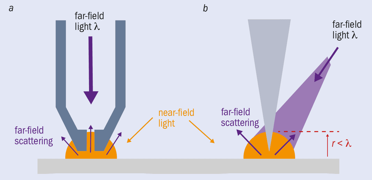
Since then, SNOM has evolved from apertures in sheets to metal-coated probes that have an aperture at the tip (figure 1a). Light can travel down a SNOM tip and out of a nanoscale aperture at the end to illuminate a sample with near-field light, which is then reflected off or transmitted through the sample. Once scattered, the light is detected as far-field. Although diffraction limited, you know where this far-field light was scattered from (the tip end) so can still achieve nanometre-scale resolution. In some systems the scattered light travels back up the tip to be detected there, and in this mode the original illuminating light can come from a separate source.
There are now also apertureless tips (figure 1b). In these SNOM systems, an atomically sharp metal tip – much like those used in atomic force microscopy – is illuminated by a far-field light source and scanned within nanometres of a sample surface, causing the near-field light to scatter and therefore be detected as far-field light. This method has the benefit of enhancing the field at the end of the tip. The light causes resonant oscillations of the electrons on the probe surface – “plasmons” – which concentrate and amplify the electromagnetic field in a highly localized area at the tip. When this enhanced near-field scatters from the sample, the interactions are intensified, producing a much greater signal that allows you to image more clearly.
Anatoly Zayats, a nano-optical physicist at King’s College London in the UK, also thinks “tipless” SNOM is possible. He works on structuring light beams with phenomena like “superoscillations” and “photonic skyrmions”, and suggests these may provide a tip-free alternative that gets around one of the technique’s main bugbears – the indispensable yet pretty much irreproducible field enhancements from the tip that greatly depend on the individual tip’s shape and size. “Even minute differences in tip size and shape might have a significant impact on the resolution,” says Zayats.
SNOM has become the workhorse for nanoscale chemical characterization, where optical spectra really give the edge over other techniques. The field enhancements that help SNOM work have spawned progress in sensing, lithography and catalysis too. Given the success you might wonder why it took 50 years for anyone to do anything with Synge’s idea from 1928, especially as his paper contained a detailed description of how to realize the instrument. Nanoscale fabrication and manipulation posed obvious challenges in the 1920s, but Zayats suggests that perhaps the most significant gap in available technology was signal collection and processing. Not only do electronics and computers now collect, store and represent image data point by point with ease, but machine learning and artificial intelligence are pushing image-processing capabilities further still. In addition, as Pohl suggests, 1928 may just not have been the right time for SNOM to take off. “The frontlines of physics were on quantum theory and the theory of general relativity,” he says, “not on such practical goals as a super-resolution imaging technique.”
Going deep
SNOM works well on surfaces, but what about a virus deep in a tissue sample? Scientists have innovated with lens and focusing systems, and found ways to exploit the shorter wavelengths of X-rays, but even as late as the 1990s the diffraction limit still held for depth imaging.
Around this time, studies of fluorescing molecules were providing molecular biologists with new tools for imaging, albeit at diffraction-limited resolutions. This set the scene for the development of a game-changing technique exploiting them. “What I realized is that it’s very hard to do anything about the focusing process itself,” says Stefan Hell, one of the directors of the Max Planck Institute for Biophysical Chemistry in Göttingen, Germany. “But resolution is about making molecules discernible. So the key to overcoming the barrier was held by the fluorescent molecule itself.”
In 1994 Hell proposed an approach for beating the diffraction limit in depth imaging based on fluorophores – molecules that can be excited to fluoresce by light at a specific wavelength but can also be suppressed from doing so with a different wavelength. Using a standard round beam to excite molecules, overlaid with a doughnut-shaped beam to de-excite them, only those molecules at the very centre, where the intensity of the doughnut beam drops low enough, will actually fluoresce. And because the doughnut beam’s intensity drops gradually towards the centre, that central region can have sub-diffraction-limit dimensions.
Hell’s experiments demonstrating “stimulated emission and depletion (STED) microscopy”, which he reported in 1999, soon inspired others. Keeping some of the molecules non-fluorescent, or working with fluorescence on–off switching using lasers with different wavelengths, turned out to be the key to “fluorescence nanoscopy”. By 2006 reports of photo-activated localization microscopy (PALM) and stochastic optical reconstruction microscopy (STORM) were also raising eyebrows. Developed by Eric Betzig at the Howard Hughes Medical Institute in the US and William Moerner at Stanford University, also in the US, PALM and STORM are both stochastic approaches (meaning they work with the probabilistic emission behaviour of fluorophores), but they differ in the types of fluorophores used. They both flood the field of view with illumination at just enough intensity to switch one fluorophore on but keep the others dark. You then need to find the emitting fluorophore with a camera and identify the centre of the molecule from the diffraction-limited intensity profile recorded. With only one molecule excited, there are no overlapping intensity profiles to confuse where the centre is.
In 2014 Hell, Betzig and Moerner were awarded the Nobel Prize for Chemistry for “the development of super-resolved fluorescence microscopy”. However, although the techniques can resolve down to a few nanometres in theory, in practice the best they manage is a few tens of nanometres. The problem is the need for more photons when you try to crank up the resolving power, whether that’s by getting as many photons as possible from the emitting fluorophore in PALM/STORM to increase the signal, or enlarging the region switching molecules off in STED. “That is limiting in terms of bleaching,” explains Hell, referring to the process whereby overexposed fluorophores can no longer fluoresce.
Recognizing the problem, Hell combined the strengths of both STED and PALM/STORM in an approach termed MINFLUX, which tracks fluorophores with a doughnut beam that excites – rather than de-excites – fluorescence. The technique homes in on an off-centre switched-on molecule by gauging its position from the measured intensity and the expected intensity profile. It uses far fewer photons and generates images with 1–5 nm resolution in just tens of milliseconds, making it possible to create movies following dynamic processes. “I think it will open up a new field for microscopy,” says Hell.
Pocket near-field optics
Imaging a structure like a virus with a resolution under 20 nm is now pretty routine in a lab setting, but optical microscopes remain bulky, complex devices. In January 2017, however, the EU launched a four-year project entitled ChipScope to design something less cumbersome.
The idea combines some of the advantages of SNOM with lensless optical microscopy, an existing technique that uses data analysis to generate images with a vastly expanded field of view based on multiple contributing images. Conventional lensless microscopes hold a sample directly under the detectors and illuminate it from a sufficient distance, which optimizes the field of view. In ChipScope, however, the sample is so close to an array of LEDs that non-diffracted near-field light illuminates it. The intensity of light transmitted through the sample is then captured by a camera as each LED is lit, to build up a shadow of the sample pixel by pixel, where each LED denotes a pixel. Although the collected light is diffraction-limited, its origin is the lit LED, and that position is known. As a result, the LED size, not the diffraction limit, determines the resolution. Before ChipScope, the state of the art for tiny LEDs was around 100 μm. Thanks to work at the University of Technology in Braunschweig, Germany, ChipScope has already demonstrated the approach with LEDs measuring 5 μm, and the plan is to push the resolution lower with 200 nm LEDs.
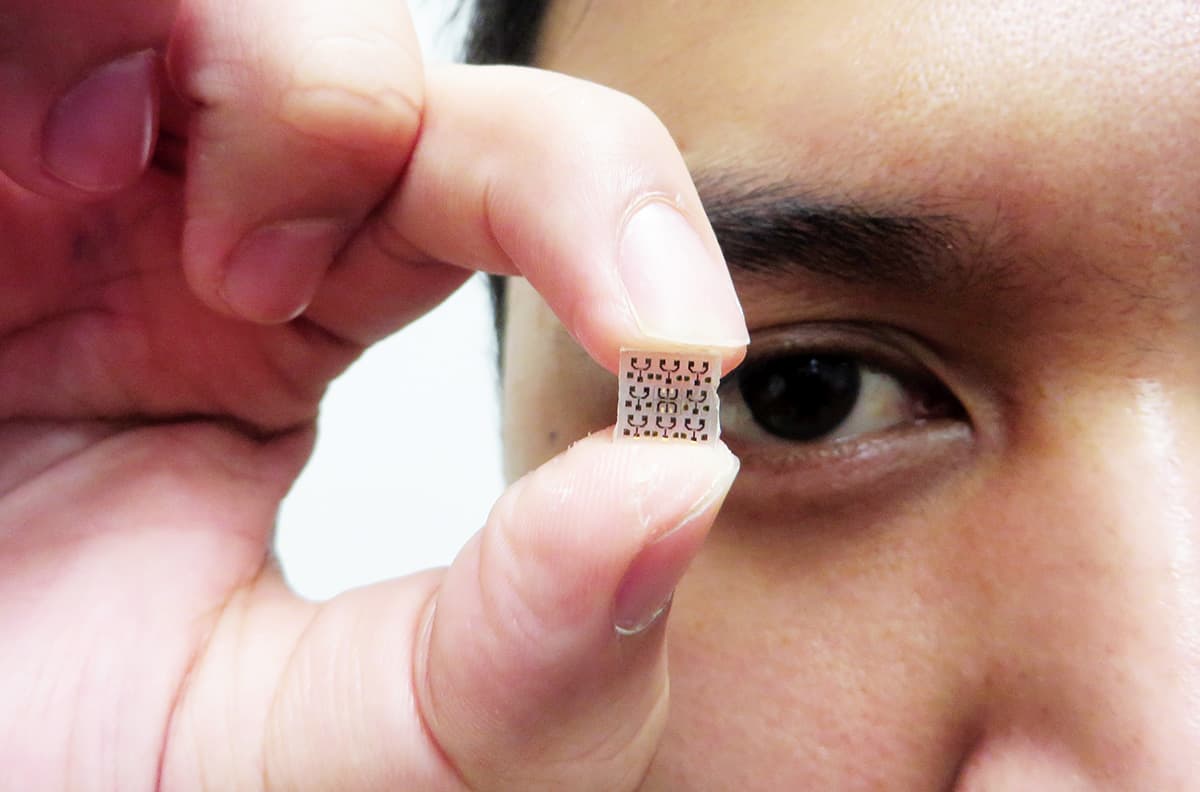
Even with 200 nm LEDs ChipScope won’t break resolution records, and so far the device is capturing intensity alone, which means it cannot be used for spectroscopy purposes. It is also limited to very thin samples – a few hundred nanometres or less – so that enough light from a 200 nm LED can pass through and is not diffracted over the thickness of the sample. But by stripping near-field optical imaging back to the bare bones, ChipScope makes huge gains in device size. Angel Dieguez, from the University of Barcelona in Spain, who is ChipScope’s project co-ordinator, describes the device based on 5 μm LEDs as proof the concept works, at least in the far-field imaging regime. “The whole microscope is half the size of a phone,” he highlights, “making it two orders of magnitude more compact than a conventional microscope.” By using 200 nm LEDs, the aim is to fit the device onto a chip that can slot into a mobile phone.
Etching 200 nm LEDs into a smooth array is no mean feat, however, and each LED needs its own wire for switching. There is also the problem of how best to operate the microscope – either by moving the sample across the LEDs with microfluidics or moving the LEDs under the sample with microelectromechanical systems (MEMS) technology. Then, somehow, you have to assemble the disparate components into a working device. Earlier this year it seemed as if the researchers had built an array of 200 nm LEDs, but the COVID-19 pandemic led to the device gathering dust in a lab as lockdown in Spain suspended further experiments. Many will be watching developments when the lab is up and running again. “It’s interesting,” says Hell, who is not involved in the ChipScope project himself. “Worth pursuing for sure.”
In the 450 years since Leeuwenhoek discovered bacteria with a single lens, countless ingenious scientific developments have shone a light on structures even smaller than viruses – in depth and even in motion. So could a fascination with phone-based nanoscopy finally subvert today’s selfie craze? Who knows, but optical microscopy’s attraction is sure to endure.