
A new paper-based semiconductor could herald the advent of sustainable electronics made entirely from plant-based materials. The material, developed by researchers at the universities of Osaka, Tokyo, Kyushu and Okayama in Japan, could be used to make sensors for wearable devices or as an electrode in a glucose biofuel cell, and could even power a small light bulb.
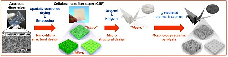
Led by Hirotaka Koga, the researchers crafted three-dimensional-network-structured semiconducting materials using cellulose nanofibres derived from wood pulp as building blocks. The result is a semiconducting paper that could be made with surface areas of more than 20 cm in diameter.
According to the team, the new semiconducting cellulose nanopaper (CNP) can be tailored for a variety of applications. The paper itself can be shaped into different designs and the material’s electrical conduction properties can be tuned from 1012 to 10–2 Ω cm – values that exceed those of previously-reported 3D semiconducting materials – by changing the concentration of charge carriers (electrons and holes) in it. This means it is suitable for use in many devices, from water vapour sensors to electrodes in enzymatic biofuel cells.
Paper folding cutting
Koga and colleagues fabricated their nanocellulose paper semiconductor from a nanocellulose/water dispersion using a combination of paper folding (origami) and paper cutting (kirigami) techniques. They also applied an iodine treatment to their material to protect its nanostructure.
To demonstrate the material’s capabilities, the researchers fabricated several differently-shaped structures, including a bird and a box by folding and an apple and snowflakes by punching out pieces of the paper. They also produced more intricate structures using laser cutting.
Photonic cellulose goes iridescent

The team say that the electrical and chemical properties of the CNP semiconductor might be altered further by modifying its molecular structure using techniques such as doping with other species of atoms. “We will be further tuning the electrical and chemical properties of the new semiconductor as well as its fine patterning,” Koga tells Physics World.
In their paper, which is published in ACS Nano, the researchers say that their study is a milestone in manipulating the functionality and practicality of semiconducting nanomaterials for various electronic applications. “As such CNP semiconductors can be prepared from ubiquitous and abundant biological resources, our strategy might be used to produce sustainable electronics,” they write.


