Physicist and engineers at Duke University in the US have developed a new metamaterial that could substantially increase the speed of wireless optical communications. The material, which consists of an array of “nanoantennas” made from cubes of silver just 60 nm wide, can capture light within a 120-degree field of view and relay it into a narrow angle with a record-high efficiency of around 30%.
Although light in the visible and infrared part of the electromagnetic spectrum carries more information per unit time than the radio waves used in wireless technologies such as Bluetooth and WiFi, data transmission at visible and infrared wavelengths is currently restricted to fibre-optic cables. One reason for this is that wireless receivers must be able to capture light from different directions simultaneously. The simplest way to do this is to make the receivers physically bigger, but that reduces the speed at which they can transmit information onwards, thus lessening any advantage.
In 2016, researchers at the Connectivity Lab (a subsidiary of Facebook) developed a new type of receiver that could, in principle, be used for wireless communications at optical frequencies. Their device consisted of a spherical bundle of fluorescent fibres that captured blue light and re-emitted green light that could then be funnelled into a small receiver. However, it could only transmit two gigabits (Gb) of information per second, which compares poorly with standard fibre-optic providers (which typically offer around 10 Gbs) as well as high-end systems offering 1000s of Gbs.
Speeding up
A team led by Maiken Mikkelsen has now used the physics of surface plasmons to speed up the Connectivity Lab’s design. Plasmons are quasiparticles that arise when light interacts strongly with electrons in a nanostructured metal, causing the electrons to oscillate collectively. By adjusting the shape, size and arrangement of the nanoscale structures, the metallic material can be tailored to capture light at specific frequencies, increasing the device’s light-absorbing speed and light-emitting efficiency by a factor of more than 1000.
Plasmonic nanocubes make an ultrafast thermal camera
Mikkelsen and her colleagues made their plasmonic metasurface by depositing an array of silver nanocubes, spaced 200 nm apart, atop a thin (75 nm) silver substrate coated with a polymer containing four layers of fluorescent dye. The researchers report that the interaction of the nanocubes with the electrons in the substrate 7 nm below enhances the overall fluorescence of the dye by 910 times and its light emission rate by 133 times. Such values were previously only possible for isolated, highly optimized single nanostructures, not for whole arrays. “While we haven’t yet integrated a fast photodetector like the Connectivity Lab did in their original work, we have solved the major bottleneck in the design,” Mikkelsen says.
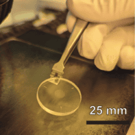
Centimetre-sized sample
The researchers also observe that the metasurface can collect fast-modulated light with a 3 dB bandwidth exceeding 14 GHz from a 120-degree field of view and relay it into a narrow angle with an overall efficiency of around 30%. This value, they say, is a record high “to the best of our knowledge”.
The researchers, who describe their experiments in Optica, say they can fabricate their metasurface over areas as large as centimetres using a simple technique known as liquid deposition without any loss in efficiency. They now plan to assemble several plasmonic devices together to cover a 360° field of view.