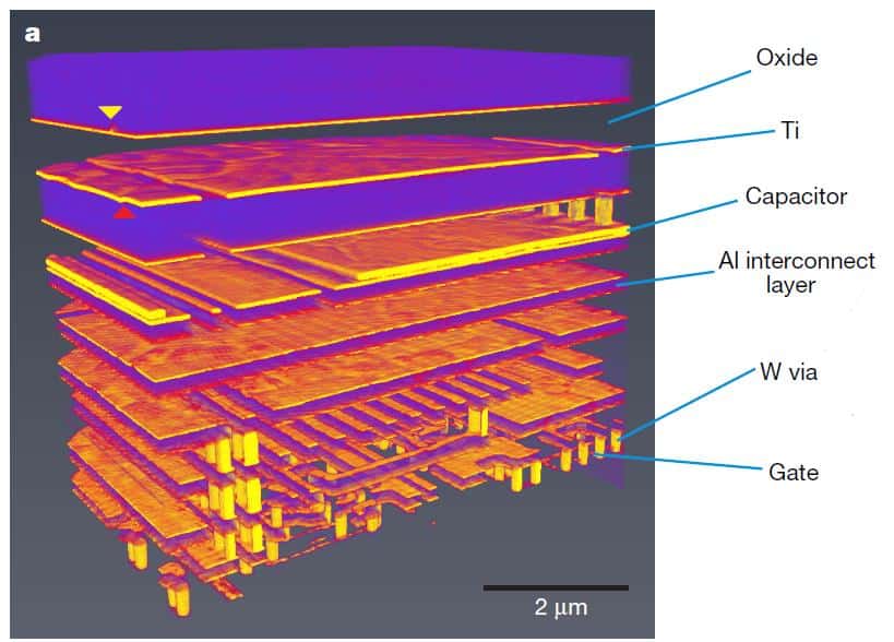
As the scale of integrated circuits (ICs) continues to shrink, the lack of practical methods for imaging their complex internal structure has hampered feedback for quality control and product development. A collaboration led by Mirko Holler at the Paul Scherrer Institut in Switzerland has published work in Nature that shows how X-rays can be used to produce 3D renderings of the internal structure of ICs with resolutions as low as 14.6 nm in all three dimensions.
Modern ICs are highly complex structures with feature sizes well below 100 nm and multiple layers of silicon, metals and silicon dioxide. Making these tiny devices is a mammoth engineering challenge, but another surprising problem faced by IC manufacturers is the ability to see what they have actually made. The current options for high-resolution imaging are atomic force microscopy, which is a surface technique and electron microscopy methods, which have a penetration depth of only a few nanometres. Seeing inside ICs currently relies on the laborious and destructive process of sectioning the device with an ion beam and imaging each layer with scanning electron microscopy.
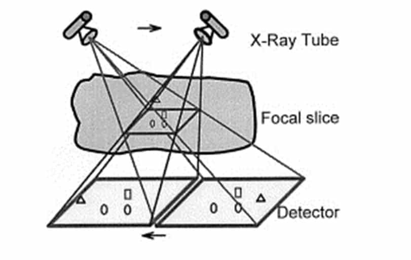
To overcome this problem, Holler’s team in Switzerland demonstrated an innovative approach using X-rays that can build a high-resolution 3D model of an IC’s internal structure. A coherent X-ray beam penetrates the sample and produces a diffraction pattern. They moved each sample to obtain several hundred such patterns, which are combined to produce a 3D model by a process known as tomography. The researchers used the so-called ptychographic scan method to obtain the diffraction patterns. This method takes 2 dimensional scans of the sample perpendicular to the X-ray beam. By using overlapping scan positions it allows the phase of the x-rays to be determined, which produces higher resolution images than is normally achievable.
Drawbacks and limitations
Although the imaging method itself is completely non-destructive, the implementations presented by the collaboration still require a destructive sample preparation process. The first example requires access to a small sample from all angles. Holler and his team achieved this by cutting out an 11 µm cylindrical pillar from the chip. However, the researchers believe that whole chips could be imaged using laminography instead of tomography. This method forms a 3D image in a series of planes by collecting diffraction patterns through the sample, thereby needing access for the X-ray sources and detectors only from above and below. To achieve this for a complete off-the-shelf chip would require a higher power X-ray source than the researchers had available. Currently, there is also a lack of scanning instruments for the method.
The other major drawback to the method is imaging speed, as a practical method must be able to image whole chips in reasonable timescales. The current system can image a 5 µm square region in just under a minute, but anticipated advances in synchrotron radiation sources and X-ray optics suggest that a 0.5 mm square region will soon be possible in the same imaging time. Synchrotron sources are available in all areas with significant IC industries, but do impose a high cost. These costs however, are considered comparable to alternative imaging methods – such as transmission electron microscopy – as well as being potentially more powerful.
Diamond Light Source – when a tool becomes a gem

The team has managed to achieve non-destructive imaging of the internal structure of an IC with excellent 3D resolution. With further development of X-ray sources and optics this promises to be a transformative technology for the analysis and quality control of integrated circuits.