Material structures are rarely perfect, but researchers at the Japan Advanced Institute of Science and Technology (JAIST) have now identified a way to make them more so. By monitoring in real time how defects called dislocations evolve in a 2D form of silicon, the researchers uncovered a way of “healing” these defects that could yield fresh insights into how to accommodate similar irregularities in other nanomaterials.
“Dislocations can strongly affect the physical and chemical properties of a crystal,” explains study leader Antoine Fleurence. “Moreover, they can undergo ‘reactions’ when, for instance, strain is applied on the crystal or atoms are added to its surface. Studying how dislocations react can, therefore, provide crucial insights on how to cure these crystal defects.”
Perfect testbed
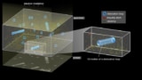
In their work, the researchers used scanning tunnelling microscopy (STM) to study a 2D layer of silicon, or silicene, placed on zirconium diboride. STM works by exploiting the tiny current which, thanks to quantum tunnelling, flows between a very sharp metallic tip and the surface of a sample that is typically kept less than 1 nm away. By controlling the distance to the sample as the tip is scanned across the surface, this current can be kept constant, and the change in the tip’s vertical position reflects the underlying topography of the surface. The technique’s spatial resolution is determined by the sharpness of the tip: if the tip terminates with a single atom, the microscope can resolve the structure of the surface at an atomic scale.
The researchers say that silicene is the perfect testbed for their experiments because it harbours an array of dislocations that disappear when a small number of silicon atoms are deposited on top of it. The challenge, explains Fleurence, is that it is impossible to predict where and when the silicene sheet will begin to transform once these silicon atoms are added.
Quantum diffusion of heavy defects defies Arrhenius’ law
A sequence of reactions
By monitoring the surface in real time for more than 24 hours – a challenge in itself, since they needed to maintain an atomically sharp STM tip throughout – the researchers were able to observe how an array of dislocations in silicene naturally accommodates the newly added silicon atoms in a way that minimizes the energy of the system. They found that the 2D material undergoes a sequence of reactions in which the silicon atoms become integrated into the silicene. Locally nucleated single-domain islands then form and propagate across the entire sheet, eventually resulting in a dislocation-free, single-domain structure. “We have now been able to observe all the steps in this process and to my knowledge, this is the first example of a dislocation reaction giving rise to their annihilation,” Fleurence tells Physics World.
While there are no direct applications for the work, the researchers say it might yield clues for how such dislocations in crystals might be healed. They detail their research in 2D Materials.