Researchers have succeeded in making the thinnest ever optical device in the form of a waveguide just three atomic layers thick. The device could lead to the development of higher density optoelectronic chips.
Optical waveguides are crucial components in data communication technologies but scaling them down to the nanoscale has proved to be no easy task, despite important advances in nano-optics and nanomaterials. Indeed, the thinnest waveguide used in commercial applications today is hundreds of nanometres thick and researchers are studying nanowire waveguides down to 50 nm in the laboratory.
“We have now pushed this limit down to just three atoms thick,” says Ertugrul Cubukcu of the University of California at San Diego, who led this new research effort. “Such a thin waveguide, which is at the ultimate limit for how thin an optical waveguide can be built, might potentially lead to a higher density of waveguides or optical elements on an optoelectronic chip – in the same way that ever smaller transistors have led to a higher density of these devices on an electronic chip.”

Cubukcu and colleagues’ waveguide is just six angstroms thick. This makes it 104 times thinner than a typical optical fibre and about 500 times thinner than on-chip optical waveguides in integrated photonic circuits.
Photonic crystal that supports excitons
The device is a monolayer crystal that consists of a single layer of tungsten atoms sandwiched between two layers of sulphur atoms suspended on a silicon frame. The researchers also patterned the monolayer with an array of nanosized holes using an ion-etching technique to form a photonic crystal that supports excitons (electron-hole pairs) at room temperature.
“These excitons generate a strong optical response, giving the crystal a refractive index that is about four times greater than that of air,” explains Cubukcu. “When we send light through the crystal, it is trapped inside and guided along the plane of the material by total internal reflection – which is the basic mechanism for how an optical waveguide works.
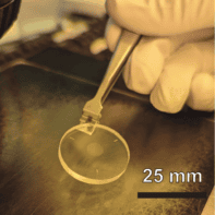
“The main challenge for us here was patterning a suspended material that was only three atoms thick,” he tells Physics World. “While the materials we employed are very robust, they can still be damaged by macroscopic forces. Happily, the students in our team devised a way to handle the structures by making use of a sacrificial photonic crystal template that they removed in the very last stage of device processing.”
Device channels light in the visible
The waveguide also channels light in the visible part of the electromagnetic spectrum – something that is challenging to do in a material so thin, he adds. Although other researchers have previously shown waveguiding in graphene (which is a sheet of carbon just one atom thick), this occurs at infrared wavelengths. “We have demonstrated waveguiding in the visible region for the first time in such a thin material.”
Another fundamental problem was to be able to probe the waveguide mode, he says. “By its very nature, a waveguide guides light in the plane of the material, but at this ultimate layer of thinness it is very difficult to distinguish the guided light from that propagating freely in space.”
To address this problem, the researchers say that they used a periodic array of holes that make use of special type of grating surface wave anomalies, known as resonant-type Wood’s anomalies, to scatter a small amount of light out of the plane of the material so that it could be detected. “As such, the light guided in the un-patterned waveguide was first coupled to the photonic crystal region and then scattered out via the Wood’s anomalies,” explains Cubukcu.
Thinnest optical resonator ever for visible light
The fact that the holes allow some light to scatter out of the plane in this way means that the suspended crystal can double as an optical resonator too, he adds.
Hyperbolic lattice appears in a coplanar waveguide array
“This also makes the device the thinnest optical resonator for visible light ever to be demonstrated in an experiment,” says team member Xingwang Zhang, who is first author of the study. “Our system not only resonantly enhances the light-matter interactions, but also serves as a second-order grating coupler to couple the light into the optical waveguide.”
Waveguides are typically used in applications in the photonics and optoelectronics industry. “For example, an optical fibre is a waveguide that forms the backbone of the Internet so we can imagine our device being used in this context,” says Cubukcu. “For the resonator, sensors might be a possible application area.”
The researchers, reporting their work in Nature Nanotechnology 10.1038/s41565-019-0519-6, say they are now looking into some fundamental research questions involving the excitons in their device. “The material we have used exhibits pronounced effects entailing these excitons so we would like to better understand these,” says Cubukcu.