A new material that is twice as magnetostrictive as others in its class could be a significant boon for computer-chip developers. The material’s unusual ability to expand and contract in response to tiny pulses of electric current has attracted interest from the chip manufacturer Intel, which is investigating possible replacements for the CMOS (complementary metal-oxide-semiconductor) technology that has dominated the industry for decades.
John Heron. Courtesy: University of Michigan
In today’s CMOS-based transistors, the semiconductor’s resistance changes when a voltage is applied across an insulating gate. This switching mechanism has long been the mainstay of electronics, remaining dominant even as transistors have shrunk down to mere nanometres in size. Reductions in the gate voltage and frequency, however, have not kept pace with reductions in chip size, and further decreases in operating voltages are unlikely because of the so-called Boltzmann limit of current control. Researchers are thus looking for alternative technologies.
Shape changes flip the magnetic field
One line of investigation concerns magnetostriction, or the tendency of an iron-containing material to expand and contract slightly as pulses of electric current are applied to it. Magnetostriction is associated with ferromagnetism and is perhaps best known as the source of the familiar hum that emanates from fluorescent lights and transformers. However, because changes in the shape of a magnetostrictive material also cause the material’s magnetic field to flip, this sometimes-irritating phenomenon could prove key to next-generation “magnetoelectric” devices.
Devices of this type would use such electrically-induced magnetic fields to store the digital one and zeros of binary data. Unlike conventional CMOS technology, these switching devices wouldn’t require a steady supply of electricity, so they should require much less energy to operate.
Unwanted order
Most magnetostrictive materials contain rare-earth elements, which are becoming too scarce and expensive to be used in the quantities required for chip manufacture. In the new work, researchers led by John Heron of the University of Michigan focused instead on an iron-gallium alloy with the chemical formula Fe1–xGax. Heron explains that the magnetostriction of this alloy normally increases with increasing concentrations of gallium. However, these increases eventually level off at around x = 19% before decreasing sharply as the higher amounts of gallium start to form an ordered intermetallic atomic structure.
To overcome this problem, the researchers used a process called low-temperature molecular-beam epitaxy to “freeze” the atoms in the compound, so preventing them from forming this unwanted order. This technique enabled the researchers to boost the fraction of gallium in the material to x = 30%, increasing its magnetostriction by tenfold compared to unmodified alloys.
“Spray painting”
Heron likens the technique, which is detailed in Nature Communications, to “spray painting” with individual atoms. The technique has a further advantage in that it allows the material’s magnetostrictive properties to be measured simply by applying it to a surface that deforms slightly when a voltage is applied.
The magnetoelectric devices in this study are several microns across, and the researchers acknowledge that this is large by today’s computing standards. However, they hope that their collaboration with Intel will help them shrink their devices down to a size that is compatible with the company’s magnetoelectric spin-orbit (MESO) device programme.
“Intel is great at scaling things and at the nuts and bolts of making a technology actually work at the super-small scale of a computer chip,” Heron says. “They’re very invested in this project and we’re meeting with them regularly to get feedback and ideas on how to ramp up this technology to make it useful in the computer chips that they call MESO.”
Heron and his colleagues have filed for patent protection on their technology through the University of Michigan’s Office of Technology Transfer.
We’ve all heard about the promise of quantum technologies to transform business and industry, whether it be for more secure communications networks or vastly more powerful computation. But what is needed to translate experimental quantum research into commercial success, and when can we expect it to happen?
According to speakers at the inaugural Quantum West conference, the transition from lab-based R&D towards market-ready solutions is already under way. While the headline-grabbing applications of quantum computing and the quantum Internet remain a longer-term bet, prototypes and products are already appearing in other areas of quantum technologies. One example is atomic clocks. Originally developed by the research community to provide more precise timing standards, the focus is now on re-engineering compact versions for use in high-speed mobile communications, synchronizing financial transactions, and other situations where accurate and resilient timekeeping offers a business advantage.
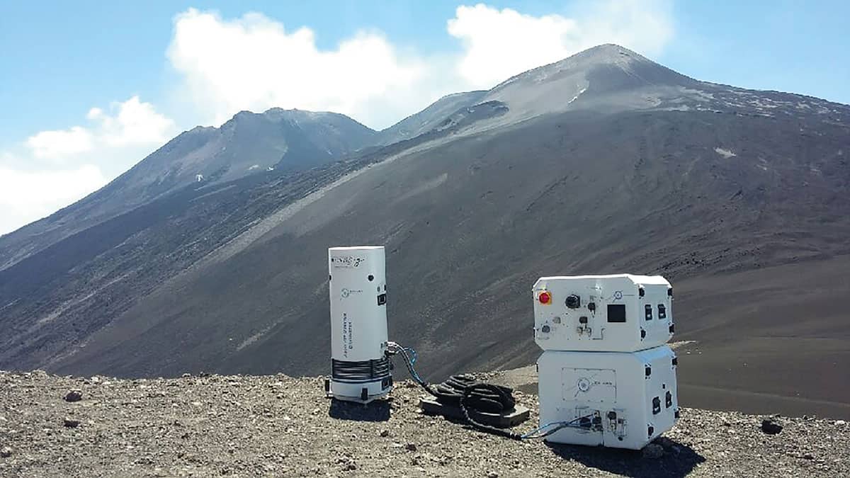
Applications for quantum sensors are also emerging. One notable example presented during the conference is a gravity sensor developed by Muquans, a French spin-off. Based on a Newtonian free-fall experiment in which a cloud of rubidium atoms cooled close to absolute zero is used as the test mass, Muquans’ system integrates all the key components into a single unit that is robust and reliable enough to be deployed in the field for geophysical monitoring – including on the slopes of Mount Etna.
“I sometimes hear the question about what will be the first real-life application of quantum technologies,” Muquans chief executive Bruno Desruelle told the Quantum West audience. “Well, there are already some quantum instruments that are in service now. We have built more than 10 units and we really believe that quantum technology offers a very interesting competitive advantage for gravity measurements.”
While the Muquans instrument is aimed mainly at the scientific community, other sensors are being developed for a mass market. As an example, the UK start-up QLM has demonstrated a gas sensor that exploits photon quantum statistics to detect methane emissions. Such a sensor could replace the manual sniffer tests currently used in oil and gas exploration to spot leaks of this greenhouse gas, and QLM chief executive Murray Reed says the company is set to produce handheld units costing less than £1000 within the next few months. The same technology could also be used to monitor emissions of carbon dioxide.
In the field French start-up company Muquans has built quantum gravity sensors based on a cold-atom experiment that is robust and reliable enough to be deployed on the slopes of Mount Etna. (Courtesy: Muquans)
Gateway to growth
The idea that early implementations of quantum systems for specific applications will pave the way for more ambitious commercial development is at the heart of the UK’s National Quantum Technology Programme (NQTP). In his keynote address, Peter Knight, who serves on the NQTP advisory board, described its approach: “We identified a kind of funnel of what we’re able to do in the very long term – for example, in quantum computing – and in the near term where we can pull out commercial and strategic value en route to achieving that long-term goal.”
The programme, which was among the first government-sponsored initiatives to recognize and encourage commercial opportunities for quantum technologies, identified four key areas where quantum technologies are likely to play an important role: sensing and timing, imaging, communications, and simulation and computing. For each area, it mapped out the commercial outcomes that could be achieved for each one over different timescales. In quantum communications, for example, a demonstrator project has already shown that quantum key distribution can be deployed in a standard fibre network, while ongoing NQTP-funded research focuses on developing quantum-resistant algorithms that will be needed to prevent attacks from next-generation quantum computers.
Matt Langione, a partner at the technology analytics firm Boston Consulting Group (BCG), delved deeper into the likely evolution of quantum computing, and its resulting market value, over the next 20 years. BCG’s analysts compared the business opportunities that more computational power would bring with the hardware and software innovations needed to deliver it – whether through improvements to classical computation or the introduction of quantum-powered solutions.
Within the next three to five years, BCG’s analysis suggests that early quantum processors with fewer than 1000 qubits, capable of tasks such as error mitigation and data compression, could deliver commercial value in four industry sectors: finance, pharmaceuticals, materials, and computational fluid dynamics simulations used in the automotive and aerospace industries. In this initial phase, Langione believes that the financial benefit for those four industries could reach a few billion dollars.
Further ahead, more sophisticated quantum computers – ones that exploit some level of error correction – will lead to a phase that Langione describes as offering a “broad quantum advantage”. Such fault-tolerant quantum computers are expected to emerge in a decade or so, and could be used in simulations that speed up materials design and reduce risk in financial trading. In the process, they might boost the overall commercial benefit to $25–50bn.
Beyond that, from about 2030, quantum computers with full-scale fault tolerance could solve the kind of problems that would completely transform the commercial outcomes from these four industries – for example by enabling the discovery of completely new drugs and materials, or allowing banks to make the most efficient use of their capital. At that point, Langione predicts that the market value generated by quantum computers would reach hundreds of billions of dollars.
Engineering a quantum future
Such views may seem optimistic, particularly when current research efforts focus on scaling up quantum processors from mere tens of qubits to the hundreds and thousands required to build fault-tolerant quantum computers. Indeed, a major emphasis of the talks at Quantum West was the urgent need to engineer practical and scalable systems for operating such complex quantum systems. Underlining the scale of the challenge was Google’s Eric Ostby, who revealed that at least 8000 additional components are currently needed to control and read out the 54 qubits in the company’s latest quantum chip.
More generally, engineering any practical quantum system will mean replacing today’s intricate experimental set-ups with robust and reliable plug-and-play units. Key to the success of the Muquans gravimeter, for example, is a bespoke laser technology that replaces optical components carefully arranged on an optical table with a solid-state frequency-doubling architecture that offers greater stability as well as easy integration with standard telecoms components.
This being Photonics West, many of the speakers focused on the crucial importance of photonics technologies for quantum applications. Lasers, for example, are widely used to manipulate quantum states, and over the last few years many devices have emerged with the narrow linewidths and wide tunability needed for quantum experiments. Even so, Scott Davis, chief executive of laser manufacturer Vescent Photonics, was candid about the shortfalls of the current generation of these devices. “There’s a gap between current laser reality and what the quantum system engineers want,” he said. “They are looking for something like a telecom package that’s cheap and fully integrated, while today’s devices only operate at certain wavelengths and are still really only designed for use in the lab.”
Part of the problem for companies such as Vescent is that there is no clear roadmap to guide their product development efforts. With this in mind, the Quantum Economic Development Consortium (QED-C), an organization that aims to support the growth of the US quantum industry, organized a workshop in September 2020 to discuss the future photonics requirements for quantum applications.
“One of the big takeaways is that the path forward for lasers for quantum is not so clear,” noted Davis, who chaired the workshop. “It’s a complicated space right now, with lots of different applications calling for different wavelengths and laser properties.” As a result, QED-C has launched an initiative to identify the technology and market intersections that should be tackled first.
Meanwhile, Davis is convinced that the best way to reduce the current market uncertainty is to get involved with academic research projects. Working in partnership with quantum scientists helps laser manufacturers to design devices that meet the specific technical requirements, from which they can engineer more integrated products that can be sold to equipment manufacturers. This has allowed Vescent to create, for example, an integrated laser-based system that has already been deployed in quantum sensors and atomic clocks.
Working together we can do so much more than working apart
Peter Knight
Many other speakers stressed the need for strong collaboration between industry, academia and government programmes to drive early commercialization efforts. This approach has already been formalized in some parts of the world, including the UK. Knight described the NQTP as building a “quantum alliance” between academic research groups (which focus on creating scientific knowledge), large and small companies (which can identify market opportunities and build practical solutions), and government (which functions as a sponsor and early adopter of quantum technologies). A measure of its success, Knight said, is that in a recent funding round for larger projects, 63 companies were involved in bids for the available £84m, and these businesses had themselves raised an additional £109m for quantum technology development over the last two years. “The appetite for working on this and translating the technology into the market is really there,” he said. “Working together we can do so much more than working apart.”
This June we will bring you Quantum Week – a series of free-to-attend scientific presentations in the field of quantum science and technology. Presentations will be on topics including quantum processors, the ethics of quantum computing and computational advantage. Find out more and register today.
Even if you’re not able to join the live events, registering now enables you to access the recordings as soon as they are available.
A bowling ball might look round on the outside, but inside there is a distinct departure from spherical symmetry. That is what I learned from reading a wonderful article on the physics of bowling balls – written by Brendan Koerner and published on the Wired website.
Called “One man’s amazing journey to the center of the bowling ball”, the article looks at the career of Mo Pinel, who revolutionized the design of bowling balls. In the early 1970’s he began experimenting with reducing the rotational symmetry of bowling balls. He first did this by drilling holes into the balls and filling them with materials with different densities. He realized that his modifications could improve how a ball was rolled but then drifted away from the idea to run a bowling-related business.
Fast forward many years later and Pinel decided to take a chance and commercialize his ideas. He created a ball with an asymmetric core that began to wobble back and forth (or flare) as it approached the end of the alley, knocking down more pins as a result. If you want to know the physics behind flaring, read Koerner’s article.
Hawking’s office
The cosmologist Stephen Hawking died in 2018 and now his archive, some personal belongings, and the contents of his office at the University of Cambridge have been acquired for the people of the UK in lieu of taxes owed by Hawking’s estate. The office contents will go to the Science Museum in London to settle a £1.4 million tax debt while the archive will go to Cambridge University Library to settle £2.8 million.
According to The Guardian, the office contents include Hawking’s personal reference books, blackboards, coffeemaker, medals and Star Trek mementoes. The Science Museum will also get six of Hawking’s wheelchairs and the technology he used to communicate after he was unable to speak. The archive includes television scripts from The Simpsons, in which Hawking appeared.
The Science Museum will display some of the items in 2022 and plans to recreate Hawking’s office
Recent advances in materials, mechanics, and manufacturing establish the foundations for high-performance classes of microfluidic lab-on-a-chip technologies that have physical properties matched to those of human skin. The resulting devices can integrate with the surface of the skin in a water-tight yet physically imperceptible fashion, to provide continuous, clinical-quality biochemical information on physiological status via capture, storage, and in situ analysis of sweat.
This webinar, presented by John Rogers, summarizes key ideas and presents specific recent examples in skin-interfaced microfluidic technologies designed for applications in sports performance, worker safety, and nutritional monitoring.
Prof. John A Rogers received his BA and BS in chemistry and physics from the University of Texas, Austin, in 1989. At the Massachusetts Institute of Technology, he completed an SM in physics and chemistry in 1992, and PhD in physical chemistry in 1995. From 1995 to 1997, Rogers was a junior fellow in the Harvard University Society of Fellows. He joined Bell Laboratories as a member of technical staff in the Condensed Matter Physics Research Department in 1997, and served as director of this department from the end of 2000 to 2002. He then spent 13 years on the faculty at the University of Illinois, most recently as the Swanlund Chair Professor and Director of the Seitz Materials Research Laboratory. In the fall of 2016, he joined Northwestern University as the Louis Simpson and Kimberly Querrey Professor of Materials Science and Engineering, Biomedical Engineering and Medicine, with affiliate appointments in mechanical engineering, electrical and computer engineering and chemistry, where he is also director of the recently endowed Querrey Simpson Institute for Bioelectronics. He has published more than 750 papers, is a co-inventor on more than 100 patents, and co-founded several successful technology companies. His research has been recognized by many awards, including a MacArthur Fellowship (2009), Lemelson-MIT Prize (2011), National Security Science and Engineering Faculty Fellowship (2012), Smithsonian Award for American Ingenuity in the Physical Sciences (2013), MRS Medal (2018), and the Benjamin Franklin Medal from the Franklin Institute (2019). He is a member of the National Academy of Engineering, National Academy of Sciences, National Academy of Medicine, National Academy of Inventors, and the American Academy of Arts and Sciences.
Scientists in the US have produced a detonation that is fixed in space for the first time. This standing wave detonation was created in a prototype engine and the researchers say that such a system could one day power aircraft at up to 17 times the speed of sound.
Most fires are deflagrations. This form of combustion creates a subsonic reaction wave and powers much of our transport technology. But you can get a much more powerful and efficient release of energy from a detonation. This type of combustion produces supersonic shock waves driven by energy release from closely coupled chemical reactions. These waves travel at many times the speed of sound, with those produced by igniting a hydrogen–air fuel mix, for example, often reaching speeds of Mach 5.
This intense energy release is highly unstable and difficult to control. If harnessed, however, it could be channelled to achieve hypersonic flight for future interplanetary travel and ultrahigh-speed intercontinental travel on Earth. Estimates suggest that an engine operating with a Mach 5 flow path, such as that produced by a hydrogen–air fuel mix, could enable vehicle speeds of Mach 6 to 17. That would allow you to fly from New York to London in just half-an-hour.
There are three main detonation engine concepts. Pulse detonation engines create repeated explosions, while in a rotating detonation engine, detonations continuously travel around a circular channel with the shockwave from each setting off the next. Both of these have been previously demonstrated. Now, researchers at the University of Central Florida and the US Naval Research Laboratory say they have demonstrated the third concept: a standing or oblique detonation wave engine. They report their results in the Proceedings of the National Academy of Sciences.
The idea behind an oblique detonation wave engine is to produce a continuous detonation that is fixed in space, so that the resulting shockwave is stable and remains in the same position. “We want to feed [the detonation] with the right propellant mixture, at the right speed and freeze it in space,” Kareem Ahmed tells Physics World.
To create such a detonation, Ahmed and his colleagues developed a prototype engine named HyperReact (high-enthalpy hypersonic reacting facility). This device is divided into three sections. In the first, the mixing chamber, a jet of hydrogen and air is ignited. This creates hot high-pressured air that flows into the next section, the converging–diverging (CD) nozzle, which has an axisymmetric square cross-section along its entire length. As the air enters the CD nozzle a jet of ultrahigh-purity hydrogen is added. The shape of the CD nozzle is designed to then accelerate the mixture to speeds of around Mach 4.5 as it enters the test section. In this final chamber there is a 30-degree turning angle ramp.
The team found that by manipulating the fuel mix, temperature and air flow through the chambers they were able to produce an oblique shock on the ramp that created a detonation that was stabilized on the ramp. This standing wave detonation lasted for the duration of active fuelling, which was around three seconds. This is significantly longer than a normal detonation and demonstrates proof-of-concept, the researchers say.
Ahmed explains that the main benefit of detonation based propulsion would be much higher efficiency than deflagration-based systems. “Achieving hypersonic speeds is critical because we don’t currently have a propulsion system that can do that,” he adds. “The only propulsion system that can give you hypersonic speeds is a rocket motor. Now rocket motors are not efficient. We know that because otherwise we’d all be flying to outer space. They are very expensive.”
Ahmed tells Physics World that now the researchers have proved that an oblique detonation wave engine is possible they want to explore the different conditions, such as fuel type and speed of the fuel flow, under which the detonation can remain stable. This is necessary to achieve the levels of control that would be required to realise hypersonic flight.
Artificial intelligence (AI) technologies are designed to replicate human capabilities, and in some cases improve upon them. Lifelike robots are physical examples of AI technology, but it is the digital AI systems that already have a ubiquitous influence on our daily lives – from facial recognition software to decision-making tools used by banks, recruiters and the police. Too often, these systems can reflect preexisting social inequalities.
In this episode of the Physics World Stories podcast Andrew Glester investigates the ethical issues that can plague AI and machine learning technologies. He finds out about the concepts of deep learning and neural networks, why these systems can amplify problems in society, and who are the people adversely affected by these flaws.
It turns out that the physics community is part of the problem and potentially part of the solution. Directly and indirectly, physicists are involved in developing AI technology so are ideally placed to raise awareness of the issues. Featuring in the episode:
Alan Winfield, a robot ethics researcher at the University of the West of England
Julianna Photopoulos, a science writer based in Bristol, UK
Savannah Thais, an experimental particle physicist at Princeton University, US
To find out more about the issue of bias in AI systems, take a look at this feature article by Photopoulos, which is summarised in the video below.
Physicists at the Massachusetts Institute of Technology (MIT) in the US have found a new way to switch antiferromagnetism on and off. Their technique, which involves doping antiferromagnetic materials with extra electrons, could allow for faster, higher-density and more stable memory storage.
Riccardo Comin, who led the research. Courtesy: Comin Photon Scattering Lab
Modern hard disk drives encode data by using magnetic field pulses to flip the spins of electrons (representing binary zeros and ones) in ferromagnetic materials within computer chips. While researchers have found ways to switch these binary bits at ever-smaller scales, the magnetic pulses require a relatively large electrical current, so the data-writing process dissipates a lot of energy. It is also relatively slow, with a complete spin flip taking tens of nanoseconds.
Promising candidates
Antiferromagnetic materials are promising candidates for future high-density memory applications because the spins in antiferromagnets flip much faster, at frequencies in the terahertz range. These rapid spin flips are possible because of strong interactions between electron spins, which come about because the spins in antiferromagnets tend toalign so that they are antiparallel to each other (unlike conventional ferromagnets, which have parallel electron spins).
Antiferromagnets also lack magnetization on the scale of a single bit (>10 nm), making them robust to external magnetic perturbations. This means that data encoded in a memory device based on antiferromagnetic bits could not be erased magnetically. A further advantage is that antiferromagnets could be made into smaller transistors (and thus be packed more densely onto chips) than is possible with conventional transistor materials like silicon.
Creating oxygen vacancies
In the new work, MIT researchers led by Riccardo Comin set out to determine whether they could manipulate the antiferromagnetic properties of 100-nm-thick films of samarium and neodymium nickel oxide (SmNiO3 and NdNiO3) by doping them with extra electrons. While doping usually involves introducing impurities in a material to alter its electronic properties, in this case Comin and colleagues achieved what’s known as carrier doping by stripping the SmNiO3 and NdNiO3 of oxygen atoms. This process leaves two electrons behind for every oxygen removed, and the left-behind electrons redistribute themselves among the remaining oxygen atoms and the nickel.
During these experiments, the researchers monitored the films using advanced magnetic X-ray crystallography techniques to determine whether the material’s magnetic structure remained intact – in other words, whether the atomic spins retained their orderly anti-alignment and therefore their antiferromagnetism. Any reduction in the previously ordered magnetic structure, they explain, would be evidence that the doping was enough to switch off the material’s antiferromagnetism.
Sharp magnetic transition
The researchers say the antiferromagnetic order in rare earth nickelates like the ones they studied is remarkably robust to carrier doping – up to a point. Then, at a critical doping threshold of 0.21 electrons per nickel atom, the order suddenly collapses. This magnetic transition is sharp, similar to switching a transistor’s state from zero to one, and can be reversed by adding oxygen back into the material.
Comin says that, like conventional ferromagnetic bits, antiferromagnetic bits might be switched using voltage gates (a process in which a small voltage is applied to a bit to alter its electrical conductivity). He tells Physics World that this would allow rare earth nickelate materials to be employed in field-effect devices that could directly read/write operations on antiferromagnetic bits.
The researchers, who report their work in Physical Review Letters, say they now hope to gain better control over the magnetic switching process, optimize it for device applications and explore more exotic physical properties in the rare earth nickelate family for functional applications. They also plan to study other materials with potentially higher magnetic transition temperatures as potential platforms for a new magnetic storage technology.
Creating a quantum computer that integrates a large number of components is a huge challenge for many reasons. One is that most quantum bits (qubits) used today must be chilled to near absolute zero and therefore isolated from the room-temperature electronic components used to control them. This makes it extremely difficult to have large numbers of qubits and controllers packed into a small space. But researchers in the Netherlands may have a solution, as the science writer and educator Karmela Padovic-Callaghan explains in this episode of the Physics World Weekly podcast.
The “wonder material” graphene is a sheet of carbon just one atom thick that has extraordinary physical properties. One promising use for graphene is to make products more sustainable. On hand to talk about how graphene can do its bit to improve the environment is Andrew Pollard, who specializes in the metrology of 2D materials at the UK’s National Physical Laboratory.
Water is another substance that has wonderous properties that have proven very useful for sustaining life on Earth. Recently, researchers used a laser technique to study supercooled water in a previously inaccessible temperature regime. Katherine Skipper, a PhD student contributor to Physics World joins us to chat about this breakthrough. Skipper also talks about her research at the University of Bristol, which is focussed on active matter that comprises two-faced Janus particles.
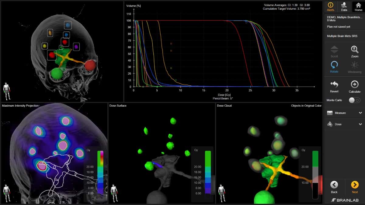
Indication-specific: Elements Multiple Brain Mets SRS dose planning enables the delivery of highly conformal single-session treatments for multiple metastases. (Courtesy: Brainlab)
Simplicity, automation, efficiency and dose targeting with sub-mm accuracy: these are the operational reference points for the radiation oncology team running the stereotactic radiosurgery (SRS) programme at Scripps MD Anderson Cancer Center in San Diego, California. Underpinning that stereotactic clinical workflow is a portfolio of enabling technologies from Brainlab, a German healthcare equipment maker specializing in hardware and software products for SRS, surgical navigation and the next-generation “digital operating room”.
“Think automated treatment planning, high-precision patient positioning plus online imaging and thermal surface guidance,” says Steve Kirsner, director of medical physics at Scripps MD Anderson. “Our established suite of Brainlab products makes it easy for physicists to do what they have to do, allowing us to deliver high-quality care to our cancer patients every time. You can’t ask for more than that.”
Kirsner, for his part, heads up a 16-strong multidisciplinary clinical team (eight medical physicists and eight dosimetrists) working across three radiotherapy centres in the greater San Diego area. Right now, those three clinics treat around 160 patients a day, with a fourth facility being commissioned ahead of coming online for initial patient treatments in August. “We run a busy SRS linac schedule for diverse brain indications,” adds Kirsner. “That’s complemented by an extensive programme of stereotactic body radiotherapy (SBRT) to treat a range of cancer types, including prostate, lung, spine, liver, pancreas and oligometastasis.”
End-to-end workflows
In developing its SRS programme, the Scripps MD Anderson team has worked closely with Brainlab engineers to implement indication-specific, end-to-end workflows for a range of brain stereotactic treatments. That specificity means the algorithms in Elements, Brainlab’s à la carte treatment planning software, are able to address the unique clinical challenges surrounding a given disease indication. Elements Cranial SRS, for example, automatically creates SRS treatment plans for complex cranial indications – including, but not limited to, vestibular schwannomas, meningiomas and large metastases – while Elements Multiple Brain Mets SRS dose planning enables the delivery of highly conformal single-session treatments for multiple metastases, minimizing dose spread to adjacent healthy tissue and critical structures.
“Elements is one of the most user-friendly platforms for SRS treatment planning,” explains Kirsner. That ease of use is particularly important when running a medical physics service across multiple sites and multiple teams. It’s straightforward, for example, to create a set of standard planning templates for a given clinical indication. Those templates can then be shared across every facility to give treatment planners a common baseline and reference point from which to develop individualized SRS plans on a patient-by-patient basis. “Put simply,” adds Kirsner, “Elements has enabled us to create a unified framework for treatment planning, driving standardization and best practice across multiple Scripps MD Anderson treatment facilities.”
It helps, of course, that Elements offers a streamlined, automated process to arrive at a high-quality SRS treatment plan, while verification of the plan and translation to the treatment machine are equally friction-free. All of which equates to a win-win for healthcare providers and patients. “Efficiency and patient throughput are key metrics for any oncology centre,” says Kirsner, “while there’s a growing demand from patients for the benefits associated with SRS treatment schedules – not least fewer visits to the clinic and a faster return to family and friends.”
Alongside Elements for treatment planning, Kirsner’s team is also taking advantage of Brainlab’s in-room X-ray-based ExacTrac positioning and monitoring system. ExacTrac X Ray enables robust verification of patient positioning – to isocentre with sub-mm accuracy – as well as intrafractional monitoring of patient motion and internal anatomical shifts during treatment. The latest iteration of the platform, ExacTrac Dynamic, is able to track patient position along an additional coordinate – using a 4D thermal camera to create a hybrid thermal image that correlates the patient’s heat signature to their reconstructed 3D surface structure.
Multiple perspectives: in addition to X-ray-based patient imaging, ExacTrac Dynamic (shown here in relation to the treatment couch) uses a thermal imaging camera to correlate the patient’s heat signature to their reconstructed 3D surface structure. (Courtesy: Brainlab)
ExacTrac Dynamic is currently being installed as part of the commissioning of the fourth Scripps MD Anderson radiotherapy clinic, with the three established treatment centres all due to upgrade to the new imaging system by the end of this year. “We like the intuitive user experience with ExacTrac,” says Kirsner, “and the fact that it allows us to image what we treat at all times, regardless of couch angle or gantry position.” In addition, the new thermal surface guidance capability will allow Kirsner and his team to automatically track both internal and external motion throughout the entire treatment of the patient. “ExacTrac imaging also integrates seamlessly with our Varian machines,” Kirsner adds. “This will allow treatment to be paused if either the X-ray imaging or surface guidance are deemed out of tolerance – so we’re excited to see the clinical impact of the latest surface-tracking functionality in ExacTrac Dynamic.”
Clinical validation
While the near-term priority for Kirsner and colleagues is the commissioning and go-live of their new radiotherapy facility, the team is also focused on achieving Novalis-Certified status by year-end. Novalis Certification is an independent accreditation programme that offers formal recognition of the highest clinical standards in SRS/SBRT treatment delivery. As such, a key outcome for cancer treatment centres is the implementation of standardized protocols for continual self-assessment and quality improvement, further reinforcing the access that Brainlab customers get to Novalis Circle, a global network of oncology centres dedicated to best practice, knowledge-sharing and collaboration on all aspects of SRS/SBRT.
“I see the independent audit of Novalis certification as a great way to strengthen the SRS/SBRT programme at Scripps MD Anderson,” concludes Kirsner. “We are all doing the best we can for our patients, but you can always learn something new from colleagues running their own radiotherapy programmes. It’s my belief that our practice here is already Novalis-compliant, so the next step is to formally document those processes and workflows for external review.”
Researchers in the US have created a new solid-state lithium-metal battery that can charge and discharge over a record-breaking number of cycles at a high current density. The proof-of-concept device, which is fundamentally different from existing liquid electrolyte lithium-ion batteries, could extend the lifespan of electric vehicle batteries to 10–15 years, similar to that of petrol and diesel cars.
The ideal battery for an electric vehicle would last a long time and store up a lot of charge very quickly. While lithium-metal batteries score well on the second of these criteria thanks to their high capacity and high energy density, their longevity leaves something to be desired. This is because, during charging, lithium ions move from the cathode to the anode. When this anode is made of lithium metal, needle-like structures called dendrites form on the electrode surface and grow into the electrolyte. Eventually, these unwanted structures pierce the barrier separating the anode and cathode, causing the battery to short or even ignite.
To overcome this problem, researchers have previously tried replacing the liquid electrolyte in these devices with a solid-state one that is more difficult for the dendrites to grow through. In practice, however, lithium dendrites can still burrow through the barrier via micron- or submicron-sized cracks produced when the battery is assembled.
Sandwich effect
Researchers led by Xin Li, a professor of materials science at Harvard University’s John A Paulson School of Engineering and Applied Sciences (SEAS), have now developed a solid-state battery in which lithium dendrite penetration is no longer a problem. Rather than stopping the dendrites dead in their tracks with a single barrier, their new battery design takes a multi-layered approach. The design, which is detailed in Nature, incorporates a less-stable electrolyte sandwiched between layers of more-stable solid electrolytes. Together, these layers keep dendrite growth under control.
The full battery “sandwich” consists of six layers: a lithium-metal anode, a graphite coating, the first electrolyte, the second electrolyte, another layer of the first electrolyte, and finally the cathode. The first electrolyte, which has the chemical formula Li5.5PS4.5Cl1.5 (LPSCI), is prone to dendrite penetration. The second electrolyte, Li10Ge1P2S12(LGPS), is more robust. The idea is that dendrites are permitted to grow through the graphite and electrolyte no. 1 but stop when they reach electrolyte no. 2 – and, crucially, before they short out the battery.
“Incorporating instability to stabilize the battery might sound counterintuitive,” says team member Luhan Ye. “But just like an (expansion) anchor can guide and control a screw going into a drywall, so too can our multilayer design guide and control the growth of dendrites. The difference is that our anchor (the LPSCI) quickly becomes too tight for the dendrite to drill through, so the dendrite growth is stopped.”
Superior cycling performance
The researchers found that when they paired their lithium metal anode with a LiNi0.8Mn0.1Co0.1O2 cathode, the cycling performance was very stable, with the battery maintaining 82% of its capacity after 10,000 cycles at a 20C rate (8.6 mA/cm2) and 81.3 % of its capacity after 2000 cycles at a 1.5C rate (0.64 mA/cm2). The design allows for a specific power of 110.6 kW/kg and a specific energy of up to 631.1 Wh/kg from the cathode material.
The test device cycled for 1800 hours at 0.25 mA/cm2, which is substantially better than the single-electrode-type batteries the researchers tested. It can also cycle at an extremely high current density of 20 mA/cm2 with a low “overpotential” (that is, the potential difference between a theoretical or thermodynamically determined voltage and the actual voltage under operating conditions) of ~0.5 V without significant signs of short-circuiting, even at a temperature of 55 °C.
Longer lifetime and faster charging
According to the researchers, the new battery technology could make the lifetime of electric vehicles comparable to that of petrol- or diesel-powered ones – 10 to 15 years – without the need to replace the battery. With its high current density, the design could also “pave the way for electric vehicles that can fully charge within 10–20 minutes,” they say.
“This proof-of-concept design shows that lithium-metal solid-state batteries could be competitive with commercial lithium-ion batteries,” Li adds. “And the flexibility and versatility of our multilayer design makes it potentially compatible with mass production procedures in the battery industry.”
The researchers say they now plan to scale up their device to a pouch cell the size of an ID card. “We expect that the attractive performance we have presented in our work will hold, since our innovation focuses on the scalable factors of materials chemistry and their combinations,” Li tells Physics World. “The design also opens the door to many new fundamental studies in solid-state battery research that were hitherto not possible without a stable lithium-metal anode.”


 Recent advances in materials, mechanics, and manufacturing establish the foundations for high-performance classes of microfluidic lab-on-a-chip technologies that have physical properties matched to those of human skin. The resulting devices can integrate with the surface of the skin in a water-tight yet physically imperceptible fashion, to provide continuous, clinical-quality biochemical information on physiological status via capture, storage, and in situ analysis of sweat.
 Prof. John A Rogers received his BA and BS in chemistry and physics from the University of Texas, Austin, in 1989. At the Massachusetts Institute of Technology, he completed an SM in physics and chemistry in 1992, and PhD in physical chemistry in 1995. From 1995 to 1997, Rogers was a junior fellow in the Harvard University Society of Fellows. He joined Bell Laboratories as a member of technical staff in the Condensed Matter Physics Research Department in 1997, and served as director of this department from the end of 2000 to 2002. He then spent 13 years on the faculty at the University of Illinois, most recently as the Swanlund Chair Professor and Director of the Seitz Materials Research Laboratory. In the fall of 2016, he joined Northwestern University as the Louis Simpson and Kimberly Querrey Professor of Materials Science and Engineering, Biomedical Engineering and Medicine, with affiliate appointments in mechanical engineering, electrical and computer engineering and chemistry, where he is also director of the recently endowed Querrey Simpson Institute for Bioelectronics. He has published more than 750 papers, is a co-inventor on more than 100 patents, and co-founded several successful technology companies. His research has been recognized by many awards, including a MacArthur Fellowship (2009), Lemelson-MIT Prize (2011), National Security Science and Engineering Faculty Fellowship (2012), Smithsonian Award for American Ingenuity in the Physical Sciences (2013), MRS Medal (2018), and the Benjamin Franklin Medal from the Franklin Institute (2019). He is a member of the National Academy of Engineering, National Academy of Sciences, National Academy of Medicine, National Academy of Inventors, and the American Academy of Arts and Sciences.