
Solar-powered water purifier is inspired by pufferfish

Pufferfish have inspired a new device that is capable of the highest rate ever of passive solar water purification – according to its creators Xiaohui Xu and colleagues at Princeton University in the US. Based on an advanced hydrogel, the system can rapidly soak up and filter water when cool, and then release clean water when warmed in the Sun. The team hopes their innovation could lead to low-cost and sustainable off-grid purification systems, potentially improving access to clean water for many communities worldwide.

According to the United Nations, one in three people worldwide do not have access to safe drinking water. Therefore, there is a pressing need for inexpensive, environmentally sustainable systems for filtering water. These are best achieved through passive purification technologies, which use solar energy to separate water from contaminants such as heavy metals, oils, and harmful microbes. Today, this is widely done by evaporating water, and condensing it onto a surface – but this is an energy intensive process, leading to slow production rates.

Xu’s team has taken a more advanced approach based on the behaviour of pufferfish. When these fish detect predators, they rapidly absorb water to swell their bodies, making themselves appear more threatening. Once danger passes, the water is quickly released. To mimic this behaviour, the researchers developed a sponge-like device they dubbed a solar absorber gel (SAG), containing three key components.

PNIPA polymer chains

At the centre of the material is an advanced hydrogel, composed of a temperature-sensitive mesh of PNIPA polymer chains, containing both hydrophobic and hydrophilic regions. At lower temperatures, these chains remain long and flexible. This enables water to flow into the mesh through capillary action, and bond with its hydrophilic regions. At temperatures higher than 33 °C, the PNIPA chains undergo a phase transition, becoming short and rigid. As a result, the mesh loses around 90% of its volume and it becomes hydrophobic – pushing water out of the material.

Surrounding this inner hydrogel is a dark layer of polydopamine, which efficiently converts sunlight into heat: enabling the PNIPA to reach its phase transition temperature in cooler conditions, while also filtering out heavy metals and organic molecules before they entered the hydrogel. Finally, an outer alginate layer filtered out any microbes, along with any other larger molecules.

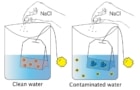
Xu’s team tested the SAG’s performance by placing it in a lake on the Princeton campus with a water temperature of 25 °C. After soaking the material, they warmed it in sunlight to release its absorbed water. Over a 2 h cycle of soaking and discharge, the material demonstrated the highest rate of passive solar water purification ever reported. The SAG was also highly durable; barely diminishing in performance even after 10 collection cycles.

Owing to their simple, water-based manufacturing process, SAG materials are low-cost and non-toxic, ensuring both their accessibility and sustainability for off-grid water purification. Xu and colleagues believe their material could be transformative: potentially improving quality of life for many communities around the world, especially where access to electricity is limited.

The research is described in Advanced Materials.

Fast electrons catch badly behaved quantum dots in the act

Quantum dots are responsible for the stunning, vibrant colours on modern TV screens, but they don’t always behave like they should. This creates headaches for device makers, who struggle to understand why some of these nanometre-scale semiconducting crystals shine much more dimly than others.

A team led by scientists at the SLAC National Accelerator Laboratory in the US has now used fast electrons to determine the cause of this bad behaviour. Their experiment – the first direct observation of its kind – probed the atomic structure of inefficient quantum dots in real time as they were (not) working, demonstrating conclusively that their inefficiency stems from energy-sapping distortions in the dots’ crystal lattice.

Quantum dots absorb light at one frequency and emit it at another. The ones in TV screens are very efficient at this, emitting almost as much light as they absorb. Their efficiency drops significantly, however, in devices such as ultraviolet photodetectors that use very energetic and bright light. Worse, when scientists try to make quantum dots brighter, the dots react by darkening instead.

Understanding inefficiency

Aaron Lindenberg, a materials-science researcher at Stanford University and a co-author on the study, explains that when quantum dots absorb photons, not all of the photon energy goes into the re-emitted light. Some of it gets wasted on processes that keep the quantum dot dark but change its properties. According to Lindenberg, pinpointing every detail of how this happens is the first step towards keeping quantum dots shining in all devices. “For a long time there has been a desire to understand the kind of microscopic processes that determine the ultimate efficiencies of these materials,” he says.

Because these microscopic processes take as little as as a trillionth of a second, they are extremely challenging to observe. The team behind the SLAC study, which appears in Nature Communications, got around this by exposing quantum dots to laser light, then firing very fast electrons at them almost immediately afterwards. By studying the way these electrons bounced off, the researchers inferred the details of the quantum dots’ atomic structure. Whenever an atom within the dot shifted, the electron ricochet pattern changed as well, providing clues as to how the shape of the dot was changing in real time.

When the laser frequency was low, the researchers found that whole dots wasted energy on warming up. With higher-frequency light, however, some of the electrons within the dots became excited enough to leave their usual places in the nanocrystal. This shifting of electrons left behind fast-moving, positively charged “holes” that travelled towards the surface of the nanocrystal. At that point, the holes got stuck, and the electric forces they exerted on the atoms around them caused the shape of the quantum dot surface to warp. In other words, the quantum dots were using the incident photon energy to contort themselves, rather than to emit light.

Caught red-handed

According to Gordana Dukovic, a physical chemist at the University of Colorado, Boulder, US, who was not involved in the study, scientists have previously speculated about the role of surface-trapped holes in quantum dot inefficiencies, but this is the first time anyone has seen these effects in action. “Trapped electrons and holes are notoriously difficult to observe,” she underscores. Her colleague Joel Eaves, who was also not involved in the SLAC study, agrees. “The fact that these researchers directly measured the lattice distortions that accompany hole trapping on the surface really is novel and impressive,” he says.

To better understand the troublesome electron-and-hole shuffle they observed, researchers also simulated the dots’ behaviour numerically. Agreement between simulations and experimental measurements strengthened the team’s hope that this new work could be used to improve future quantum dot technologies, notes Dmitri Talapin, a chemist at the University of Chicago, US and co-author on the study. Now that they have experimentally determined what kinds of photons lead to energetically costly distortions and hole trapping within the quantum dot, they can try to minimize these effects. “By tuning the colour of the light that you use to excite these nanocrystals, one could potentially control these processes that, in the end, are detrimental,” Lindenberg explains.

Though such fine-tuning may not be needed for TV screens, it could make ultraviolet photodetectors more efficient or even lead to creation of new types of lasers built out of quantum dots. Talapin adds that though quantum dots are similar to traditional semiconductor technologies – a sort of smaller cousin to, for example, silicone-based devices – their size gives them different properties, making them promising candidates for future devices that might rely on absorbing energy from photons. “There is a strong consensus between the academic community and industrial communities that this class of materials sort of presents an interesting competitive platform as semiconductors 2.0,” he says. The experiment he and his collaborators conducted is a step towards making quantum dots an even stronger competitor in this field, he concludes.

Independent QA and the necessity of data access

Want to learn more on this subject?

This webinar will address the critical role of independence in providing unbiased assurance in radiation therapy that treatment-related issues are caught. While vendor-integrated system self-checks represent some efficiency gains, independent quality assurance and the data accessibility required for it remain essential – especially as treatment complexity increases.

In this webinar, presented by Jeff Kapatoes, you’ll hear about:

  • Defining data access for Radiation Therapy Quality Management and what access enables.
  • What is gained from independent checks, including avoiding bias error, avoiding conflicts of interest, complementing evolving treatment complexity and encouraging continuous improvement.
  • Reviewing guidelines and published findings that highlight independent checks for Patient QA and Machine QA.

Want to learn more on this subject?

Jeff Kapatoes received his PhD in medical physics in 2000 from the University of Wisconsin as part of the tomotherapy research team. Upon graduation, he joined start-up TomoTherapy Inc, spending 10 years with the company, culminating with his management of the software development team, which included responsibility for treatment planning, optimization, database services, treatment delivery, imaging and calibration. Kapatoes then worked at Mevion Medical Systems as the director of project management and helped the company secure its initial FDA 510(k) clearance. In 2012, he joined Sun Nuclear Corporation as the product manager of its Patient QA products. He continues to work for Sun Nuclear today as the senior director of research and regulatory.

Human hand used as an infrared source to reveal secret messages

The human hand can be used as an infrared radiation (IR) source to decrypt hidden messages and register sign-language-style finger gestures, researchers in China have shown. The concept could find application in anticounterfeiting and gesture-driven control of devices.

The human body, like all matter, emits thermal radiation – specifically at infrared wavelengths (IR). While invisible to the naked eye, this emission can be seen using thermal imaging cameras and some night-vision goggles. The emissions from individual parts of the body are small but significant. An average hand, for example, puts out around 4 W of infrared power with an intensity of some 212 W/m2 – compared with 0.6 W and around 823 W/m2 for a standard LED.

In their study, materials scientists Tao Deng and Wen Shang of the Shanghai Jiao Tong University and colleagues set out to see if the low-level emissions from the human hand could be captured and put to a practical use.

Secret pattern

To this end, they took an aluminium surface – which has a high IR reflectivity – and stencilled on a pattern using a mix of hexane and polydimethylsiloxane, which has a low IR reflectivity. Under ambient light, the image they created is not discernible to the either human eye or an infrared camera. This situation changes, however, when the infrared light from a hand is shone over the secret pattern.

“When there is no hand, the coding pattern, including both the region of low IR reflectivity and region of high IR reflectivity, is in temperature equilibrium with the background,” the researchers say, explaining that the IR radiances from different regions are the same, resulting in no contrast between the pattern and the aluminium background.

However, they add, “when the human hand is used as the light source, the IR emission from the hand is reflected by all the regions, and thus, the region of high IR reflectivity has a higher increase of IR radiance than that of low IR reflectivity.” As a result, the pattern stands out to an infrared detector.

Encrypting information

By varying the depth of the polydimethylsiloxane layer, the team found that they were also able to varying the infrared reflectance of the pattern in specific areas – with thicker applications resulting in more absorption of the radiation and therefore a lower reflectivity. In this way, the team were able to encrypt more information into the pattern.

“The IR camera can automatically assign colours to the IR image to characterize the level of IR radiance from different areas,” Deng explains – meaning that the team are able to deposit patterns that, when processed can be turned into colourful images of flowers or patterns of human fingerprints and random shapes that might be used for unclonable security coding.

The system does have one limitation: as the ambient temperature rises (or one’s hands get colder), the reflectivity contrast decreases. The team propose a simple solution for this however – which is to rub your hands together to increase their temperature to compensate.

Individual digits

In the final part of the study, the team note that the movement of individual digits can effectively turn the human hand into a “powerless and multiplexed infrared light source”, one in which “the relative position and number of light sources are controllable and adjustable at will by changing hand gestures.” By combining an infrared camera with various specially tuned diffraction gratings, the team propose that a system could be set up to decipher hand gestures, either to serve as a form of passcode or to allow contact-less control of a device.

“This is an interesting proposal and it is surprising that there is a discernible difference in the IR propagation from individual fingers. I would have thought that each digit would behave as a Lambertian emitter and so the spatial information would become lost at relatively short distances,” comments Howard Snelling – a physicist at the University of Hull who was not involved in the present study. Noting that the human hand is technically powered (“albeit by food!”), he adds: “It will be interesting to see if the detection system can be developed to simplify this scheme as much as the hand has for the source. Currently, the use of an IR camera adds considerable cost and reintroduces the need for external power.”

With their initial study complete, the researchers are now looking to both optimize the performance of their decryption and control systems, alongside explore new potential applications – especially within the field of human–machine interactions.

“Apart from sign language recognition [we demonstrated], this technique may also be used in human machine interaction for other applications – such as virtual game, virtual reality, smart home and office, vehicle control, and healthcare and medical assistance,” Deng says.

The study is described in Proceedings of the National Academy of Sciences.

Metallic glasses reveal their secrets

A highly detailed plot that shows, for the first time, the location of all 18 356 atoms in a metallic glass nanoparticle could transform our understanding of non-crystalline materials. The feat, achieved thanks to a technique known as atomic electron tomography (AET), could also make it easier to design materials with properties suited to applications in quantum computing and gravitational wave detection.

Metallic glasses were discovered in 1960 and have properties of both metals and glasses. They contain metallic bonds, so are conducting, but their atoms are disordered like in a glass rather than ordered as in a crystal. They are produced by heating certain substances to above their melting points and then quenching them in a way that prevents them from crystallizing, and their exceptional strength makes them promising for structural engineering applications. However, their disordered nature makes it difficult to study their three-dimensional structure using crystallography techniques. While alternative methods – including X-ray and neutron diffraction, high-resolution transmission electron microscopy and nuclear magnetic resonance – are available, none of these can directly identify all the positions of the atoms in 3D.

Atomic electron tomography

In a paper published in Nature, Jianwei Miao of the University of California, Los Angeles, US, and colleagues note that AET can, in principle, solve this long-standing problem. The technique works by passing a beam of electrons through a sample to acquire 2D projections of its 3D atomic structure. From there, a series of 2D images is obtained by changing the orientation of the sample with respect to the beam. In a final step, the images are reconstructed into a 3D image of the entire sample.

AET has previously been used to image 3D crystal defects (such as dislocations, stacking faults, grain boundaries, chemical order/disorder and point defects) in materials at the single-atom level. Obtaining the 3D atomic structure of a metallic glass, however, required two important advances, Miao says. “We optimized our experiment to expose a sample to the lowest possible ‘dose’ of electrons needed to generate images to avoid changing the sample during the course of the measurement,” he tells Physics World. “We also developed advanced algorithms to analyse the noisy images and then stitch them together to obtain a 3D map.”

After years of pursuing their goal, Miao and colleagues say they finally succeeded in analysing a series of high-quality 2D images that capture subtle variations in contrast when the metallic glass is viewed in different orientations. They then used their advanced algorithms to map out the precise 3D position of 18 356 atoms in a metallic glass nanoparticle (see this video).

Crystal-like superclusters

The team, which also includes researchers from the Lawrence Berkeley National Laboratory and the University of Maryland, studied metallic glass nanoparticles containing eight elements: cobalt, nickel, ruthenium, rhodium, palladium, silver, iridium and platinum. They classified these into three different atom types: cobalt and nickel as type 1; ruthenium, rhodium, palladium and silver as type 2; and iridium and platinum as type 3.

The researchers quantitatively characterized the short- and medium-range order of the 3D arrangement of the atoms. They observed that, although the short-range 3D atomic packing is geometrically disordered, some short-range-order structures connected with each other to form crystal-like superclusters, giving rise to medium-range order.

Miao and colleagues identified four types of crystal-like medium-range order (face-centred cubic, hexagonal close-packed, body-centred cubic and simple cubic) that coexist in the amorphous sample. These observations back up the so-called efficient cluster packing model for metallic glasses.

The team also showed that some of these clusters are densely packed, while others are looser. The loose packing might stem from the process in which the glasses were synthesized, but it might also hint at important gaps in current models.

In a related News & Views article, Paul Voyles of the University of Wisconsin, Madison, US, notes that AET could open the way to better ways of characterizing structural defects in glasses. Technologies as varied as the superconducting quantum bits used in quantum computers and certain optical coatings used at the LIGO gravitational-wave observatory could benefit as a result, as both are currently limited by glass defects known as two-level systems. These defects can be detected only by their spectroscopic signatures, not by their structure, Voyles explains, so being able to identify them more readily could make it easier to design better materials for these and other applications.

Spinning black holes can be deformed by tidal forces, calculations reveal

Some spinning binary black holes can tidally deform as they merge together – according to new calculations by Alexandre Le Tiec at the Observatory of Paris, and Marc Casals at the Brazilian Centre for Research in Physics. The duo has shown that supermassive black holes will tidally bulge as stellar-mass bodies spiral into them. The results offer new guidance for future measurements of the gravitational waves emitted by such black hole mergers.

In strong gravitational fields, rigid bodies including planets will deform. The effect can be quantified using three “tidal Love numbers” (TLNs), which describe how an object will deform when subject to tidal forces. Scientists are keen on measuring TLNs because they encode crucial information about the internal structures of massive bodies – including the compositions of planets and exoplanets. The same mathematics can be used to study deformations of merging neutron stars, which can be observed using gravitational waves. This has allowed astronomers to place constraints on the deformations of merging neutron stars.

The situation, however, is not clear with black holes. Previous calculations have shown that within static gravitational fields, non-spinning black holes should display no deformation at all. Yet since all black holes are believed to rotate to some degree, it has remained unclear whether this assumption holds for mergers in which tidal fields caused by the mutual attraction of the black holes are asymmetric around each black hole’s rotational axis.

Tiny bulge

Through new theoretical analysis, Le Tiec and Casals predict that tidal bulges can indeed occur during mergers. For a black hole spinning at 10% of its maximum possible rate in an asymmetric tidal field, their calculations show that tidal bulges can appear, with a corresponding quadrupolar TLN of 0.002. In comparison, the quadrupolar TLN for a much more deformable Earth is 0.3, while a neutron star has a number of about 0.1.

While this means that black holes must be far more rigid than planets and neutron stars, the duo predict that their deformation should be enough to influence merger dynamics. For example, in the case of a stellar-mass black hole spiralling into a supermassive black hole potentially billions of times more massive, the resulting tidal bulge in the larger object would generate a torque, slowing down its rotation. In turn, the effect may influence the properties of the gravitational waves produced when the black holes merge – although this would be far too subtle to detect with the current LIGO–Virgo gravitational detectors.

Le Tiec and Casals hope that the situation could change with the ESA’s Laser Interferometer Space Antenna (LISA) mission, with a planned launch date of 2034. As the first space-based gravitational wave detector, the probe will enable astronomers to place constraints on black hole deformation roughly 8 orders of magnitude more stringent than current ones on neutron stars. Using the duo’s theories to study these future results, astronomers could gain important clues about the compositions of the most massive bodies in the known universe.

The research is described in Physical Review Letters.

Copper nanowire foams filter tiny airborne particles

Copper nanowires that have been transformed into a foam can filter submicron-sized airborne particles with over 96.6% efficiency. The material, which is lightweight, resistant to chemicals and easy to clean, reuse and recycle, could be used in face masks as well as air cleaners to help fight the COVID-19 pandemic, according to the researchers at Georgetown University in the US who developed it.

In a study published in Nano Letters, Kai Liu and colleagues note that the current COVID-19 health crisis has highlighted the crucial role of submicron-sized airborne particles and particulates in the spread of infectious respiratory diseases. The virus that causes COVID-19, SARS-CoV-2 (severe acute respiratory syndrome coronavirus 2) is itself very small and measures around 0.1 μm across.

Ultrafine particles are a problem

When a person infected with the virus exhales (and especially if they also sneeze or cough), they release viral particles into the air. These particles are often attached to much larger droplets. Droplets and particles bigger than 2.5 μm generally have limited reach because they rapidly precipitate thanks to gravity. However, objects below this size (denoted as PM2.5), such as aerosolized viral particles, can remain suspended in the air for hours or even days and travel long distances, spreading the virus as they go. Ultrafine particles, 0.3 μm or smaller (PM0.3), are even more dangerous since they can penetrate deep into the respiratory system, with some even reaching the bloodstream.

The fibres on the surfaces of face masks bind these small particles to the mask via van der Waals forces. Charged fibres go a step further, binding the particles via electrostatic interactions. The problem is that the polymeric fibres typically employed in highly efficient particulate air (HEPA) filters and N95 face masks tend to degrade when exposed to UV radiation, solvents or chlorine-based solutions. This makes it hard to decontaminate and reuse them. The filtering efficiency of fibres that trap particles electrostatically also dramatically decreases once the masks become moist and the fibres discharge. Another important concern is the sheer volume of plastic-based waste currently being generated around the world in the form of used face masks.

Metallic foams are efficient filters

Researchers recently discovered that metallic foams might be effective filters for submicron-sized airborne particles. As well as being structurally robust – even to high temperatures and pressure – such materials are resistant to various organic solvents, corrosive chemicals and even UV radiation.

In their new work, Liu and colleagues fabricated metal foams by casting copper nanowires made using an electrodeposition technique into a free-standing three-dimensional network. They then solidified the structure by sintering it. Finally, they applied a second layer of copper (again using electrodeposition) to further strengthen the material.

Excellent filtering for a broad range of particle sizes

The extremely large surface area of the foams makes them excellent filters for a broad range of particle sizes, including PM0.3. Indeed, the Georgetown team found that they efficiently filtered particles across the 0.1 to 1.6 μm size range. This is particularly relevant for fighting COVID-19, as aerosolized viral particles in this size range are most challenging to capture, they say.

The most effective material they made was 2.5 mm thick and contained 15% by volume of copper. This foam trapped 97% of 0.1-0.4 μm aerosolized salt particles (which are commonly employed to test face masks) without the use of electrostatics. The breathability of the foams was generally on a par with, or even higher than, commercially available polypropylene N95 face masks (as tested using pressure differential measurements).

The researchers say the foams can easily be cleaned by rinsing them with water or blowing compressed air at them. And since the new material is based on copper, it should be recyclable and resistant to chemical-based cleaning products too. Copper is also naturally antimicrobial, so it should destroy viruses trapped on the filter surface.

The materials would currently cost around $2/mask, according to the researchers’ calculations, a figure that could be reduced further with mass production on an industrial scale. The fact that they can be disinfected and reused would also help make them economically competitive with currently-available products.

“Our results demonstrate a new type of efficient particulate filter, especially for submicron-size particulates such as the SARS-CoV-2 virus, and could potentially be used in face masks,” Liu says. “We now plan to explore a number of other filtration mechanisms that may further improve the foam’s filtration efficiency and enhance new functionalities in prototype filtration systems,” he tells Physics World.

Whitest paint ever could keep your house cool, space fridge could store better food for astronauts

One way to keep cool this summer is to coat your roof with what is claimed to be the whitest paint ever made. Created by engineers at Purdue University in the US, the coating reflects 98.1% of sunlight – shattering the previous record of 95.5%, which is also held by the team led by Xiulin Ruan.

What is more, the paint is a good emitter of radiation at wavelengths that pass very easily through the atmosphere, which reduces the temperature of the coating via a process called radiative sky cooling. This means that the coating can be cooler than the surrounding air.

According to the team, a painted roof of about 9 m2 could deliver a cooling-power equivalent of about 10 kW – which is greater than a typical domestic central air conditioning system.

Seasonal problem

This is one catch, however, if you live in an area with cold winters. The team points out that at 6 °C the paint surface can be a chilly -4 °C, so the paint could increase your heating bills.

One solution would be to paint your roof black in the autumn, perhaps using Vantablack – which incorporates carbon nanotubes to absorb 99.9% of visible light.

Purdue University must be a very cool place to be because researchers there have also joined forces with Air Squared and Whirlpool Corporation to develop a refrigerator for use in space. While fridges for experiments and biological samples operate on the International Space Station (ISS), they are not very energy efficient and therefore not practical for food storage. As a result, astronauts tend to rely on canned and dried food with a shelf life of about three years. Fridges could extend the lifetime of stored food by another three years and also increase the range of food that can be stored.

While the vapour-compression fridges used in kitchens on Earth are very efficient, they rely on gravity to keep the liquid and vapour phases of the refrigerant in the right places. Similarly, the motor driving the system is lubricated using a gravity-based system.

But now, Leon Brendel and colleagues have developed a refrigeration system that does not rely on gravity and should operate in microgravity environments such as the ISS. In their lab, they have shown that the fridge will operate upside down – or at any angle, for that matter.

Parabolic flights

The next step is for Brendel and four other members of the team is to fly with their fridge on parabolic flights run by the company ZERO-G, which uses a specially outfitted A310 to create a microgravity environment for about 22 s.

“This is a once-in-a-lifetime opportunity for me. I can’t wait to board the plane,” says Brendel in the video above.


Synchrotron characterization of buried interfaces in solid-state batteries

Want to learn more on this subject?

Transportation accounts for 23% of energy-related carbon dioxide emissions and electrification is a pathway toward ameliorating these growing challenges. All solid-state batteries could potentially address the safety and driving range requirements necessary for widespread adoption of electric vehicles. However, the power densities of all solid-state batteries are limited because of ineffective ion transport at solid–solid interfaces.

New insight into the governing physics that occur at intrinsic and extrinsic interfaces are critical for developing engineering strategies for the next generation of energy dense batteries. However, buried solid–solid interfaces are notoriously difficult to observe with traditional bench-top and lab-scale experiments.

In this talk, Kelsey Hatzell will discuss opportunities for tracking phenomena and mechanisms in all solid-state batteries in situ using advanced synchrotron techniques. Synchrotron techniques that combine reciprocal and real-space techniques are capable of tracking multi-scale structural phenomena from the nano- to meso-scale.

This talk will discuss the role that microstructure plays on transport and interfacial properties that govern adhesion. Quantification of salient descriptors of structure in solid-state batteries is critical for understanding the mechanochemical nature of all solid-state batteries.

Want to learn more on this subject?

Kelsey Hatzell is assistant professor of mechanical engineering, assistant professor of chemical and biomolecular engineering, and Flowers Family Dean’s Faculty fellow in engineering at Vanderbilt University. Her research focuses on printable materials and understanding electrochemistry at interfaces as well as solution-processed material synthesis of low-dimensional materials for energy storage and water desalination application. She earned her BS/BA in engineering/economics from Swarthmore College; MS in mechanical engineering from Pennsylvania State University, US; and PhD in material science and engineering at Drexel University, US. Hatzell has received research awards including the Sloan Fellowship in Chemistry (2020), POLiS Award for Excellence (2021), MRS Nelson “Buck” Robinson Science and Technology Award for Renewable Energy (2019), ECS Toyota Young Investigator Fellowship (2019), Oak Ridge Associated Universities (ORAU) Ralph E Powe Award (2017), and NSF CAREER Award (2018). She was also a Scialog research fellow in energy storage and negative emissions technologies. She joins the faculty of Princeton University School of Engineering and Applied Science and the Andlinger Center for Energy and the Environment (ACEE) in the fall.

Twist direction influences electron behaviour in magnetic bilayers

The electrons in certain magnetic bilayer materials behave very differently depending on whether the two layers are twisted left or right with respect to each other. This finding from researchers at East China Normal University in Shanghai could shed fresh light on so-called moiré systems and aid the development of new two-dimensional materials for optoelectronics and perhaps even energy storage devices.

In 2018, scientists at the Massachusetts of Technology (MIT) showed that “twisted” bilayer graphene – made by stacking two sheets of graphene on top of one another, and then rotating one of them so that the sheets are slightly misaligned – could support a wide array of insulating and superconducting states, depending on the strength of an applied electric field. When placed on top of each other in this way, the graphene sheets form a moiré pattern, or superlattice, in which the unit cell of the two-dimensional material expands as though it were artificially stretched in the two in-plane directions. This expansion dramatically changes the material’s electronic interactions.

Twist angle

The twist angle in twisted bilayer graphene in important. The MIT study, for example, showed that at an angle of 1.1°, the material switches from an insulator to a superconductor, capable of carrying electrical current with no resistance at temperatures below 1.7 K.

In the new work, researchers led by Chun-Gang Duan studied a particular crystalline phase of vanadium diselenide, 2H-VSe2. This material belongs to a family of bilayer transition-metal dichalcogenides (TMD) designated 2H-MX2, where M is a transition metal and X is a chalcogenide such as sulphur or selenium. Using first-principle calculations on a twisted supercell of this material, the Shanghai team found that the material responds very differently to an applied external electric field depending on whether the sheets are right- or left-twisted with respect to each other at an angle near 30°.

Rare effect

The researchers explain that this exotic property stems from the electrons in the sheets redistributing themselves according to the direction in which the lattices are stacked.

When an external electric field is applied to a neutral atom, an electric dipole (a pair of negative and positive charges) usually forms. The induced dipole moment, or polarization (which is defined as pointing from the negative charge towards the positive charge with a size that equals the strength of each charge multiplied by the separation between the charges) generally points in the same direction as the external field.

In the case of right-twisted 2H-VSe2 sheets, however, no apparent electric dipoles form when an electric field is applied. In the left-twisted case, electric dipoles do form, but the induced polarization can even align in the opposite direction to that of the applied field – an effect that is very rare in nature.

“Since this is a novel magnetoelectric property, there could be many possible applications,” Duan tells Physics World. “These include energy storage devices, negative capacitors and new-generation optoelectronics.”

The researchers, who report their work in Chinese Physics Letters, say they now hope to detect such magnetism-mediated dielectric polarization in laboratory experiments.

Copyright © 2026 by IOP Publishing Ltd and individual contributors