Water-based batteries enable a green energy future

A cheap, safe, and effective potassium-ion battery system with promising characteristics has been described in a Nature Energy article by Yaxiang Lu, Yong-Sheng Hu and co-workers in Beijing, bringing the renewable energy grids of the future closer to the realization.

Green energy storage

One of the obstacles to total green energy reliance is that many sources of carbon-neutral energy, such as solar and wind power, are unpredictable and intermittent. A possible solution is to build energy storage facilities that can charge up while excess energy is being generated, then discharge when demand overtakes supply.

Battery-based grid-storage facilities using a range of battery types have already been built for this reason, but there is still a need to develop an economical, safe, and long-term solution. Li-ion systems such as the 129 MWh Hornsdale power reserve are the current state of the art, benefiting from high energy density of Li-ion batteries. Na-S cells are a close competitor (e.g. the 300 MWh Buzen substation), having excellent energy density and low cost. Both of these battery types use highly flammable parts which increases their cost due to safety considerations.  The main goal is optimizing the cost per MWh over the whole lifetime of the battery, for which non-flammable aqueous battery systems are a tempting prospect. They may also be manufactured more cheaply on larger scales than other batteries, which require rigorously dry conditions.

Novel materials

The cathodes in the cells Lu and Hu et al. demonstrated are more stable than in other systems, retaining 90% of their energy storage capacity after 10,000 cycles. One reason for their stability is that part of the distortion prone manganese in the Prussian Blue (KxFeyMn1 − y[Fe(CN)6]) material is substituted with iron. Another reason is the use of an electrolyte containing more potassium salt than water, to inhibit the dissolution of the cathode material over its long life. The anode used in the cells, an organic paint pigment (PTCDI), also has the potential to be manufactured cheaply.

The most remarkable feature of the cells was their tolerance of high rates of charging and discharging, comparable to Li-ion battery performance, without losing much of their capacity. Although the overall energy density of the cells is moderate, due to their comparatively low voltage of 1.3 V, there is potential for optimization in this system, both in increasing the voltage by adjusting the cathode metal and anode composition, and by lowering material costs to produce a very low cost per MWh system.

Delignified wood could help cool down buildings

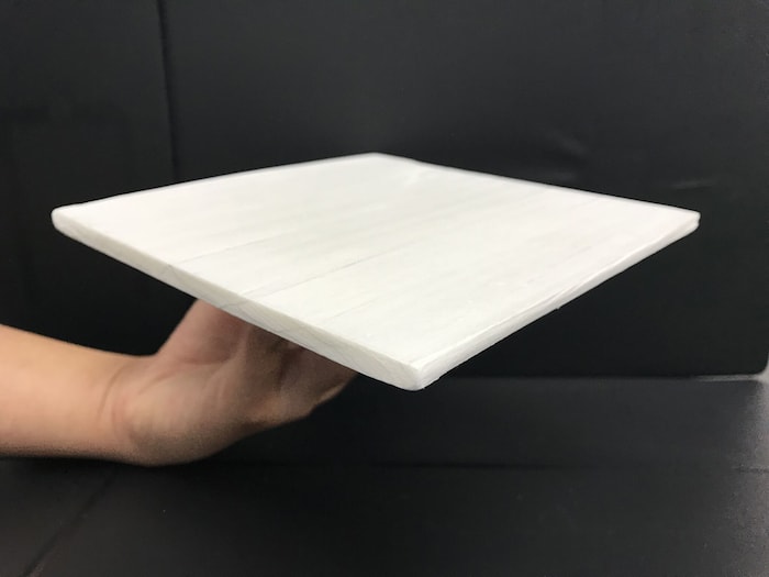
A new passive radiative “cooling wood” that reflects infrared radiation could reduce the energy costs associated with cooling buildings by between 20 and 60%. The material, which is more than eight times stronger than natural wood, is made by removing the lignin from wood and then compressing the delignified structure.

“Buildings account for more than 40% of the total energy demand and 70% of electricity use in the US, leading to an annual energy bill of more than $430 billion,” explain Liangbing Hu of the University of Maryland and colleagues. “Heating and cooling accounts for roughly 48% of this energy use, making it the largest individual energy expense.”

Cooling a building is generally more difficult than heating it. Passive radiative cooling materials, which cool a structure by deflecting incoming solar radiation and dissipating heat with no external energy input, have come along in leaps and bounds in recent years, but these can be difficult to manufacture on a large scale.

Wood has been used in construction for thousands of years and has recently emerged as an important sustainable building material that could replace steel and concrete. Hu and colleagues engineered their cooling wood by completely removing the element that absorbs solar radiation, lignin, from it.

Cellulose nanofibres strongly emit light in the infrared

Scanning electron microscopy images reveal that the wood contains cellulose nanofibres that do not absorb in the visible part of the electromagnetic spectrum. These multiscale fibres and the channels between them in fact act as random and disordered light scattering elements at all visible wavelengths. At the same time, the molecular vibration and stretching of cellulose molecules in the wood strongly emit light in the infrared at all angles from the surface of the material in the so-called first and second atmospheric transparency windows of 8 to 13 μm and 16 to 25 μm respectively. The result is that the heat flux emitted by the material is greater than the absorbed solar irradiance, which leads to passive cooling.

The wood's natural nanostructures

The researchers measured the Fourier transform infrared absorbance of their wood and found that the strong infrared emission at wavelengths of 8 to 13 μm comes mainly from the complex infrared emission of OH groups on the cellulose together with C-H, C-O and C-O-C stretching vibrations between 770 and 1250 cm-1. The strongest IR absorbance by OH and C-O centres is at around 1050 cm-1 (9 μm). 

Good radiative cooling powers

The team, which includes scientists from the University of Colorado Boulder, the University of California Meced and Huazhong University of Science and Technology in Wuhan, tested the performance of the wood in Cave Creek, Arizona, using continuous thermal measurements on samples measuring 200 x 200 mm placed 12 metres above ground (to avoid heat conduction from the ground to the samples).

The researchers found that the wood had radiative cooling powers of 63 and 16 W/mduring the night and daytime (between 11 o’clock in the morning to 2 pm) respectively. This leads to an average cooling power of 53 W/mover the 24-hour period.

Continuous sub-ambient cooling

“Our wood is capable of continuous sub-ambient cooling – that is, keep its surface cooler than ambient air temperature,” says Hu. “It also features an exceptional tensile mechanical strength of as high as 404.3 MPa and a toughness of 3.7 MJ/m3, values that are, respectively, eight and 10 times tougher higher than those of natural wood.”

The material also has a specific tensile strength (the ratio of mechanical strength to weight) of 334.2 MPa cm3, which is higher than that of most structural materials, including Fe-Mn, Al-C steel, magnesium, aluminium alloys and titanium alloys, he adds. It requires no energy input either and could thus be a sustainable material for improving the energy efficiency of buildings.

The new building material

Modelling potential energy savings

The researchers, reporting their work in Science 10.1126/science.aau9101, modelled the potential energy savings of using their cooling wood on the exterior surfaces of buildings using the whole building energy simulation program EnergyPlus version 8 and parameters listed in their paper. This model accounts for a total heat balance on both the internal and external building enclosure surface, the heat transfer through the building enclosures and heat sources and sinks, they explain.

The building models employed in this study are midrise apartments in 16 cities in the US and include both old (built before 1980) and new (built after 2004) buildings. The energy modelling process established a baseline energy consumption for these buildings and then recalculated this by supposing that the building materials had, in part, been replaced by the cooling wood.

We determined the total cooling energy-saving patterns for the selected 16 cities and the percent savings relative to the baseline and found that found that an average of ~35% and ~20% in cooling energy savings can be obtained for old and new midrise apartment buildings, respectively, say the researchers.

The energy savings that come from installing the cooling wood on the exterior surfaces of these buildings show that Austin (22.9 MJ/m2), Honolulu (28.2 MJ/m2), Las Vegas (21.1 MJ/m2), Atlanta (17.1 MJ/m2), and Phoenix (32.1 MJ/m2) would have the highest energy savings among the selected 16 cities. Phoenix had the highest because of its hot and dry climate.

“We conclude that the Southwest may be the area to benefit the most from this material to reduce energy consumption for cooling,” says Hu. “Indeed, UMD spinoff company Inventwood LLC in Maryland is now commercializing this technology,” he tells Physics World.

Minibeam radiotherapy: from photons to charged particles

Dose distributions

Advances in the technologies used to deliver radiation therapy have enabled improved tumour conformity along with reduced dose to nearby organs-at-risk. However, the dose tolerance of normal tissues remains a limiting factor in radiotherapy dose delivery. This leads to difficulties in treating radioresistant tumours, for example, or cancers near highly sensitive structures, such as paediatric brain tumours.

One option could be to employ new modes of radiation dose deposition, for example, delivering spatially fractionated dose using an array of submillimetre-sized radiation beams. At the recent ESTRO 38 meeting in Milan, Yolanda Prezado from CNRS described the rationale for this novel approach.

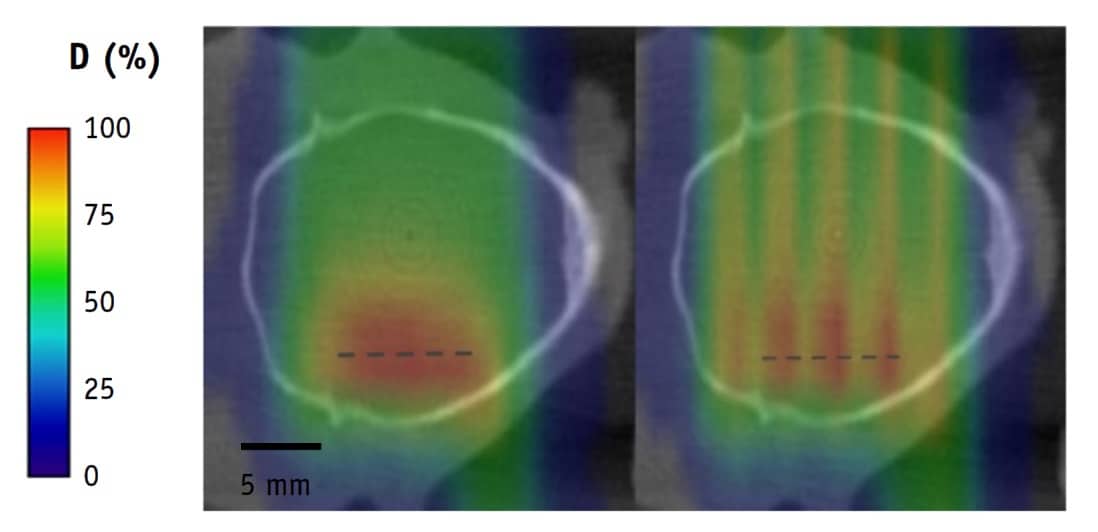
In its most extreme, she explained, microbeam radiotherapy uses beams of around 50 µm in width spaced by a few hundred microns. This creates an inhomogeneous dose distribution with alternating high peak doses and low valley doses. When using such radiation beams, normal tissue can withstand doses as high as 300 Gy in one fraction. However, such small field sizes and high dose rates can only be created by synchrotron sources.

“This concept is fascinating, but clinical trials are very difficult because these very high dose rates are confined to synchrotrons,” said Prezado. “Instead, it may be a good compromise to use minibeam radiotherapy.”

Minibeams have a width of between 500 and 700 micron, and can be produced by lower-cost equipment other than synchrotrons, allowing a more widespread implementation. Prezado described a proof-of-concept study demonstrating that such minibeams still provide normal tissue sparing in glioma-bearing rats compared with conventional radiotherapy. As well as eliminating normal tissue damage, the minibeams also increased tumour control, she noted.

Moving forward, Prezado introduced a newer concept: proton minibeam radiotherapy (pMBRT). In a first evaluation of this approach, Prezado and colleagues compared whole-brain irradiation of glioma-bearing rats with either standard proton therapy or pMBRT, both using a prescription of 25 Gy in one fraction (Int. J. Radiat. Oncol. Biol. Phys. 10.1016/j.ijrobp.2019.01.080).

They found that the standard treatment caused skin damage and substantial brain damage in the animals. Treatment with pMBRT, however, which delivered a peak dose of 58 Gy, resulted in no skin damage and a net reduction in toxicity. The minibeam treatment also increased the animals’ long-term tumour-free survival, from 22% to 67%.

“This is among the best results ever obtained with radiotherapy alone, and with a reduction in neurotoxicity,” Prezado noted.

She suggested that pMBRT could provide a novel radiotherapy concept to solve an urgent medical need, namely the ability to increase the tolerance doses of normal tissues. This, in turn, could reduce the risk of complications in paediatric cancer therapy, enable dose escalation to treat radioresistant tumours, and even reduce costs by enabling hypofractionation and reducing targeting requirements. Preparations for the first clinical trials are starting, she told the delegates.

Another potential approach for the future could be to employ minibeams of heavy ions. Prezado explained that ion beams of 500 µm in width can be generated and that using a large beam spacing minimizes the contribution of high-LET fragments to the valley dose, generating an extremely high peak-to-valley dose ratio. She noted that a dosimetric study had shown that heavier beam fragments are dominant in the valleys only at the target position, which may help increase tumour control.

Prezado concluded by pointing out that the dose delivery method may impact the tumour’s biological response — and may actually be more important than the dose level itself. “I think that for clinical practice, it’s a good choice to fully exploit spatial fractionation,” she said.

Tiny optical clock is 100 times better than previous chip-based timekeepers

A tiny optical clock that is small enough to fit onto three computer chips has been created by physicists at the National Institute of Standards and Technology (NIST) in Boulder, Colorado.

The next-generation device is 100 times more stable than current chip-based atomic clocks of a similar size. With further improvements, the tiny timekeeper could have a diverse range of both scientific and commercial applications.

For over six decades the most accurate timekeeping devices have been atomic clocks – the best of which could run for more than one billion years before being out by just one second. Most commercial atomic clocks operate by monitoring the frequency of microwaves emitted by a certain transition in a caesium atom. However, the best atomic clocks use transitions that emit  light – which has a much higher frequency than microwaves. As a result, these optical clocks are much more accurate that their microwave counterparts. The downside, however, is that optical clocks are bulky, complex, and expensive – limiting their use to labs such as NIST.

Infrared transition

NIST researchers are keen to simplify optical clocks and put them on chips so that they can find wider application. Their design is based around a microfabricated glass vapour cell filled with rubidium atoms, which have a transition at 385 THz. While this is not quite visible light – it is in the infrared – it is much high frequency that the caesium transition at 9 GHz.

An infrared “clock laser” is locked to the rubidium transition. Two interlocking Kerr-microresonator frequency combs are used convert the terahertz clock laser time signal into a gigahertz frequency, which is widely used by standard electronics.

The simplicity of this design meant that the clock could be incredibly compact. It fits onto just three small chips, but it does require supporting electronics and optics. Using just 275 mW of power, the device showed an instability of just one part in 1013 after operating for 4000 s. This makes it around 100 times more stable than current atomic clocks of a similar size. With further improvements, the NIST team believes that their optical clock could become small enough to be handheld, making it highly competitive with current atomic clocks.

If optical clocks become small, portable, and inexpensive enough, they would be suitable for a range of commercial applications, including timing and navigation when GPS is unavailable. It would also open up new opportunities for scientific experiments, including gravitational and remote sensing, long-baseline interferometry, and calibrations of lab instruments; potentially allowing for new tests of fundamental physics.

The clock is described in Optica.

  • One of the NIST researchers, John Kitching, spoke about the lab’s drive to put atomic clocks and other metrology devices on chips in this episode of the Physics World Weekly podcast.

Condensing droplets get a boost from micron-thin polymer coating

A new surface coating that could boost the efficiency of refrigerators and other industrial systems that rely on condensers has been developed by Kripa Varanasi and colleagues at the Massachusetts Institute of Technology. The thin polymer layer can be deposited on a range of different surface shapes and materials to enhance the formation and shedding of low-surface-tension droplets. Their discovery could ultimately increase the efficiency of a wide variety of large-scale industrial processes by almost 2%, creating a significant dent in their greenhouse gas emissions.

Condensation plays an important role in many large-scale industrial processes including refrigeration, liquification, waste heat recovery and distillation. Unlike water vapour, which condenses on a cold surface producing droplets that coalesce and quickly drip away, many industrial substances (such as ethanol and hexane) have a much lower surface tension. Instead of forming droplets, these liquids will spread out across the surface of a condenser in a process called wetting. This forms an insulating layer that limits heat transfer and therefore inhibits the operation of the condenser.

In their study, Varanasi’s team set out to combat this problem by creating a surface on which the low-surface-tension substances would form droplets, which would coalesce over time before dropping-off under gravity. To do this, the researchers first developed a technique for depositing a thin polymer coating onto surfaces, without inhibiting heat transfer itself. This involved a technique called initiated chemical vapour deposition (iCVD), in which a surface reacts with a gaseous polymer to create a micron-thick solid layer.

Titanium and steel

Varanasi and colleagues used iCVD to deposit polymer layers onto a wide variety of substrates, including both flat and pipe-shaped surfaces of steel and titanium. In each case, they observed droplets forming readily on the surfaces and little evidence of wetting. What is more, the droplets coalesce and were eventually shed under gravity.

Since iCVD is a relatively simple process, the team says that it could be used to create large, industrial-scale components. Furthermore, iCVD could be used to retrofit existing equipment, thereby minimizing costs. As well as being durable even in high wear-and-tear industrial environments, Varanasi’s team says that their deposited polymer could allow for anywhere between a four- to eightfold improvement in heat transfer. Ultimately, this would equate to a 1.8% improvement in the overall energy efficiency of some industrial systems – which they say is a significant increase that could help in the ongoing fight against climate change.

Varanasi says that the coatings could play a useful role in systems based on the organic Rankine cycle – which are used for generating power from waste heat in a variety of industrial processes. “These are inherently inefficient systems,” he says, “but [iCVD] could make them more efficient.”

The research is described in Joule.

Atom patterning breaks new number record

Neutral atoms trapped by light in arrays of dipole traps could be used as quantum bits for quantum computing. For such applications, however, these atoms must be positioned individually within the traps to create defect-free arrays that can then be used in information processing. Researchers at the Technische Universität Darmstadt in Germany have now developed a new technique for patterning 111 atoms in this way, so breaking the previous record, set last year, of 72 atoms. The method should even be scalable to one million atoms or more, they say.

In their experiments, the researchers, led by Gerhard Birkl, began by creating a cloud of several million rubidium atoms in a room-temperature vacuum system using a magneto-optical trap. They then cooled the atoms down to around 100 microKelvin and transferred these atoms into a microtrap array, which consists of hundreds of laser traps arranged in a square lattice. They made this lattice by directing a laser beam through an array of commercially-available microlenses.

One atom per trap

At first, each trap contained a few atoms but Birkl and colleagues succeeded in generating patterns consisting of trap sites that contained either one or no atoms. They did this using a technique called collisional blockade to remove pairs of atoms from each site. Those initially containing an odd number of atoms were left with one, and those containing an even number with zero.

Next, the researchers took an image of the pattern, which allowed them to identify the occupied and empty sites. They then filled each empty site by picking up a single atom from a filled site outside the target pattern and transporting it to an empty site inside the pattern.

“We acheived this using a single focus laser beam that we can move in 2D throughout the whole trap array,” explains Birkl. “The process is like using tweezers made out of light, which is why they are called ‘optical tweezers’. These were invented by Arthur Ashkin in 1986, who received part of the 2018 Nobel Prize in Physics for his work.”

Multiple assembly processes

Once they had filled all the empty sites in this way, the team then took another image of the atoms’ distribution to determine how successful their process to generate defect-free atom patterns was. “In case our control program saw any empty sites left, we repeated the assembly process one more time,” says Birkl. “Indeed, we can repeat it up to 80 times in one experimental run, which is another reason for why we can successfully create large-defect patterns.”

The technique can produce 10×10 atom squares, a checkerboard containing 105 atoms and two interconnected squares containing 111 atoms.

“The large number (361) of currently used traps, the corresponding large number of close to 200 single atoms as a resource and the large number of repetitions of the assembly process we can apply are key to breaking the previous number record of 72,” adds Birkl. This number could be further increased to one million thanks to the microfabricated microlens arrays used in this work. “In our lab, we already have systems containing close to 10 000 lenslets and the technology to generate lens patterns with up to 1 000 000 lenslets already exists. We could approach this number with enough available laser power and improved experimental apparatus.”

Scalability will be key

The research is important for many subfields of quantum technology, including quantum simulation, quantum computing, quantum measurement or even atomic clocks, he tells Physics World.

“Pivotal to further progress in all of these fields is the scalability of the physical systems employed. In quantum computing, for example, the large number of atomic qubits we could create using our technique will allow us to realize large-scale quantum memories. And quantum error correction, which is a key element in any practical quantum computer, will be possible since we can store one bit of quantum information simultaneously in many physical quantum bits.”

The researchers, reporting their work in Physical Review Letterssay they would now like to scale up their system to 1000 atoms – to start with. “We will also work on initiating two-qubit quantum gates between the atoms to build a 2D quantum processor based on so-called Rydberg interactions,” reveals Birkl, “and implement large-scale quantum entanglement and quantum simulation.”

How permanent summer time could affect your sleep, BBC sings the praises of kinetic theory

There is a plan afoot in Europe to do away with the annual switches between standard time and summer time (or daylight-saving time, as it is known in North America).

Tonight in Bristol (at about 51° latitude) the Sun will set at 9:08 pm and on the June solstice it will be daylight until 9:31 pm. I think most would agree that it would be crazy to give up these long, bright evenings – so I’m hoping that, if the UK does stop changing its clocks, it will remain on summer time all year round.

The downside to being on summer time all year round is that it would not be light until 9:13 am in Bristol on December 21 if the UK remained on summer time. This worries some because it would mean that children would have walk to school in the dark for much of the winter.

José María Martín-Olalla is a physicist based in Spain who has devoted much thought to the effects of changing clocks. Perhaps this is because Spain is effectively always on summer time (or indeed double summer time at the moment). This is because despite being at roughly the same longitude as Britain and Ireland, Spain keeps the same time as its more easterly continental neighbours.

In the above video Martín-Olalla, looks at how sunrise and sunset times affect sleep patterns at different locations around the world.

The development of the kinetic theory of gases in the 19th century was a triumph of physics that has sadly been forgotten – in part because it was quickly followed by relativity and the quantum revolution. That is the gist of the latest episode of the BBC’s In Our Time radio programme, which looks back on how physicists and chemists managed to get a handle on the physics of huge numbers of molecules whizzing around in a gas.

You can listen to the discussion here.

Battle of the elements: what makes carbon King of the Elements?

What links the Earth and the air? What both sparkles like starlight and reflects almost nothing at all? What underpins the chemistry of biological molecules – life itself – and has launched a whole field of materials science in 2D, not to mention its mechanical, electrical and optical properties, which are worth (to funders at least) billions? In some form or another carbon and carbon compounds take a piece of the action in almost all fields of science.

So what makes carbon so ubiquitous in so many fields? A chemist might think a good place to start is by looking at how carbon bonds to other elements. As a physicist by training, though, I’d add that where it gets really interesting is explained by physics.

Carbon atoms comprise a nucleus of neutrons and six protons surrounded by six electrons. Quantum mechanics dictates that the first two electrons occupy the inner atomic orbital, while the remaining four electrons have wavefunctions that only half-fill the second standard and three second principal orbitals. This leaves each carbon atom hungry to bond with other atoms. Hydrogen aside, there are more compounds of carbon than any other element, and these include the whole of organic chemistry.

Chemical promiscuity

The most basic organic molecule is methane – one carbon atom bonded to four hydrogen atoms. The tetrahedral shape formed by the four hydrogens gives each of carbon’s outer electrons as much distance as possible from the others – like some siblings who are too similar to enjoy each other’s company. Lop off a hydrogen and stick two together and you get ethane; add yet another methyl group and you get propane, and so on.

What makes organic chemistry so prolific is the ready substitution of the bonds to hydrogen atoms for bonds with other atoms and molecules, as well as double or even triple bonds. For example, replace a hydrogen with an oxygen bonded to a hydrogen on the other side and you get an alcohol. The alcohol of ethane is the ethanol found in beer, wine and spirits. (Some might argue that alone makes carbon King of the Elements).

If you replace the OH in ethanol with a chlorine atom, and string several of those units together, you get polyvinylchorine (PVC), an example of a huge branch of organic chemistry, polymers. The range of properties that can be achieved with polymers has led to a whole industry in plastics – materials so stable, cheap and versatile that governments across the world are struggling to keep up with Mumbai in regulating their proliferation and disposal.

Strings of carbon also form rings, like benzene – a ring of six carbons where each carbon is bonded to two other carbons on either side and a hydrogen. It took a while for people to figure out what was going on with the fourth outer electron until a model was established for a shared, or “delocalized”, electron orbital around the carbons of the ring. (These delocalized π orbitals crop up in another carbon structure that has been taking materials science by storm.) These rings and their derivatives – aromatic compounds, after benzene’s strong fragrance – further enrich the library of organic compounds.

A cycle for life

A rich source of hydrocarbons that are either used as fossil fuel or the precursors for other industrial chemicals is crude oil, formed when carbon-rich plants and animals decompose under certain conditions deep in the bowels of the Earth. Burning oil and other fossil fuels releases carbon dioxide, as does the breathing and regular decomposition of living animals at more moderate rates.

Plants then use CO2 from the air in photosynthesis to grow, part of the cycle of carbon from air to plant to other organisms that maintains the balance between different chemicals in the atmosphere. The vast quantities of CO2 currently released in fossil-fuel combustion is knocking this balance out of kilter, prompting growing demand for alternative energy generation and storage technologies, and energy efficient devices.

All that does not glitter…

Even with the whole of organic chemistry among the carbon compounds, some of the most fascinating materials science – and  the inspiration for technologies with applications from medicine and computer science to alternative energy generation and storage – is when carbon bonds only with itself.

In diamond the carbon atoms bond with each other in a regular tetrahedral lattice. This giant covalently bonded structure makes diamond extremely hard and stable to high temperatures as well as exposure to other chemicals. The lattice also gives diamond its sparkle, although disruptions to the crystal lattice aren’t all bad.

I remember my disappointment when samples arrived for some of my friends studying diamond for their PhDs. They were just little brown squares with no sparkle at all, because of defects in the crystal that have dazzled researchers in different ways. For example, nitrogen-vacancy defects – where a nitrogen substitutes for a carbon atom next to an empty lattice site – give rise to electron spin behaviour that researchers have been looking to exploit in applications ranging from microscopy and quantum computing to bioimaging.

Layers of interest

Unlike diamond, other forms of carbon are conducting. As far back as the17th century, people were using a conducting form of carbon in one of the most ubiquitous data storage tools on the planet – the pencil. The graphite running through pencils has a layered structure and each layer is a honeycomb lattice, like tessellated benzene rings where each carbon atom is now bonded to three nearest neighbours. As in benzene, a delocalized π orbital forms, allowing electrons to flow through the structure.

Of course, a pencil does not exploit graphite’s conducting properties, but it works because the covalent bonds between the layers of graphite are weak and a little friction against a sheet of paper is enough to rub off layers and record data in a written trail. Researchers have also exploited these weak interlayer bonds in graphite substrates that can be easily cleaned by removing the top layer with a piece of sticky tape. Thanks to the curiosity of Andre Geim and Kostya Novoselov in their legendary Friday night experiments on these discarded bits of sticky tape, the phenomenal properties of a single or very few layers of carbon – now known as graphene – have been keeping researchers and funders busy for over a decade since, and will likely continue to do so for decades to come.

Even before the discovery of graphene by Geim and Novoselov at the University of Manchester in 2005, studies of carbon nanotubes – discovered in 1990 by Sumio Iijima – had given a glimpse of the kind of mechanical and electronic properties that emerge from a single layer of carbon. One of the attributes of graphene that has excited researchers recently is the way the properties of materials comprising more than one layer of graphene can be tuned by the presence of other 2D materials, and even by the angle or twist between graphene layers themselves. And I would bet my hat that there is more to discover in other forms of nanocarbon in the future.

So we literally live, eat and breathe carbon. It feeds our industries, inspires our labs, and is the cause and potential solution to some of the greatest challenges facing the planet. Carbon is so ubiquitous across living organisms that radioactive measurements of the carbon composition can be used to date them – so carbon owns time too. Be it work, rest or play there is nothing you can do that carbon does not influence, govern or facilitate. Like it or not, carbon is King of the Elements.

  • This article was edited to clarify the shape of the methane molecule and diamond crystal lattice units 7th June 2019

What’s your favourite element? Contact us at pwld@ioppublishing.org with your pick – and the reason why – or via Twitter using the hashtag #battleofelements.

Reducing air travel does not impact academic productivity, claims study

Flying to ever-more far-flung scientific meetings and locations does not make you a more productive scientist with better citations on your papers. That is the claim of a study that examines the relationship between air-travel emissions and various measures of academic success. Carried out by researchers at the University of British Columbia (UBC), in Canada, the study suggests that academics can therefore take steps to reduce flying without fear that it will impact their academic output.

Scientists travel for many reasons such as carrying out experiments, attending conferences, giving lectures as well as visiting colleagues — all of which are considered important for academic success. But researchers are increasingly questioning the value of such travel. “Academics tend to fly quite a lot and we are living in a carbon constrained world,” says UBC researcher Seth Wynes. “There is a limited amount of carbon we can put into the atmosphere if we want to stay within a safe temperature for our planet, so it is really important we reduce how much we fly.”

To measure the impact of frequent flying on academic success, Wynes and colleagues looked at the travel of 700 academics from eight UBC departments over an 18-month period. The data came from travel-request forms that provided the team with details such as trip duration, airport codes, number of flights in a trip, ticket class and reason for travel. This information also allowed the researchers to estimate the greenhouse gas emissions for each trip.

Most travel was to attend conferences (60%), with the rest classified as being fieldwork (16%), miscellaneous and unreported purposes (13%), university business (6%) and lectures (5%). The team classed 5–10% of the air travel as avoidable – such as a same-day return, a one-night long-haul trip or a short trip that could have used other modes of transport. And up to a quarter of journeys were considered to have produced avoidable emissions, either because the air travel itself was avoidable or that academics sat in a class higher than economy (Journal of Cleaner Production 226 959).

A cultural shift

When the researchers compared the academic performance of 128 academics — for whom the necessary data was available — with their work-related air-travel emissions, they found no relationship between emissions and the author’s “h-index” – a measure of a researcher’s productivity and impact of their publications. No connection was found even when the h-index was adjusted for academic age and discipline. There was also no correlation between air travel and the average number of authors on a paper – usually taken to be a sign of collaboration.

There was, however, a difference when the h-index was adjusted for academic age and discipline for full-time faculty that appeared to have not flown at all during the study period. “We found that researchers in our sample who didn’t fly at all had lower scholarly outputs than those who did fly, but among those who did fly – once you took at least one trip in our 18-month sample – then there was no relationship, doing five trips was not better than one,” says Wynes.

Wynes told Physics World that he doesn’t think the work shows that academics cannot attend conferences, but that there are a lot of trips that might be unnecessary. “It might be that we can get away with fewer trips – we can reduce our emissions – and still be successful,” he says. As well as a cultural shift among academics, Wynes says that institutions can also help to reduce flying by taking steps such as providing better video-conferencing equipment, software and facilities as well as changing promotion requirements to ensure they are not incentivising international trips. “A lot of institutions are already taking progressive action on this,” he adds. “It is very exciting to see.”

Turning microfluidic devices into mini-centrifuges

The team

Microfluidic or “lab-on-a-chip” devices are commonly used to analyse blood and other fluid samples, which are pumped through narrow channels in a transparent chip the size of a postage stamp. These chips can be used to culture cells that are grown to mimic specific organ function and investigate the basic mechanisms of physiology and disease. For example, current efforts focus on studying how organs react to drugs and developing point-of-care diagnostic tools for various diseases. However, across these different applications, the design of the chip channels remains roughly the same, with innovation mainly coming from the composition of the surrounding cell layers or the addition of sensors.

Enter Khashayar Khoshmanesh and the interdisciplinary Mechanobiology & Microfluidics research group from the Royal Melbourne Institute of Technology (RMIT), who engineered a cavity the size of a grain of sand along the channel to enable new ways of analysing cells and particles (Adv. Funct. Mater. 10.1002/adfm.201901998).

Moulding a cavity

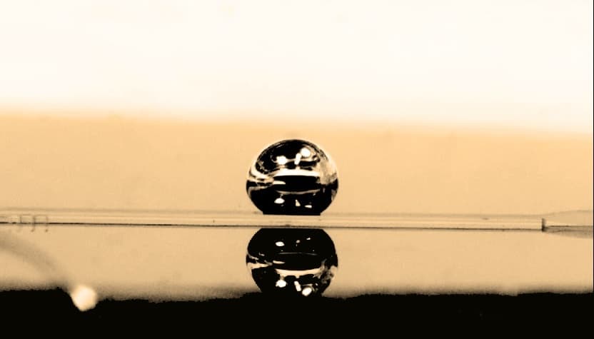
The team took advantage of gallium-based liquid metal alloys that can display properties of both metals and fluids. The researchers added droplets of the alloy Galinstan onto a chip that was then covered with the traditional polydimethylsiloxane (PDMS) layer and left to cure for 48 hours. Galinstan’s high surface tension means that it holds its form during the moulding process.

Liquid metal drop

At the end of this process, they injected sodium hydroxide solution into the PDMS to release the Galinstan droplets and used a pipette to remove both the released droplets and the solution, producing an empty microfluidic structure with this novel cavity.

The spherical cavity left by the droplet acts as a mini-centrifuge — when a liquid is injected into the channel, it enters the cavity and spins around within. “This spinning creates a natural vortex, which just like a centrifuge machine in an analytics lab, spins the cells or other biological samples, allowing them to be studied without the need for capturing or labelling them,” reports Sara Baratchi, co-lead on the study.

The device only requires tiny samples, as little as 1 ml of water or blood, and can be used to study tiny bacterial cells measuring just 1 µm up to human cells as large as 15 µm.

Potential applications beyond blood sample analysis

The team performed numerical simulations to study the effects of various parameters — such as the size of cavity or flow rates — on the vortex magnitude and shear stress, as well on particles leaving the cavity to re-enter the channel. In this way, the researchers mimicked the response of blood cells under disturbed flow situations, similar to that found at junctions and curvatures of coronary and carotid arteries.

But mimicking human physiology on a chip is not the only potential application for this technology. It could also be used to identify parasites and other infections in waterways, especially in developing countries where options to detect and filter water impurities are scarce. “But with this device, the impurities will be captured and orbited by the vortex without any special sample preparation, saving time and money,” says Khoshmanesh.

Combined with a smartphone capable of capturing high-speed images, this new microfluidic device could prove to be a low-cost, self-sufficient and portable point-of-care diagnostic device.

Copyright © 2026 by IOP Publishing Ltd and individual contributors