From eyeglasses to space telescopes, lenses play crucial roles in technologies ranging from the mundane to the cutting edge. While traditional refractive lenses are a fundamental building block of optics, they are bulky and this can restrict how they are used. Metalenses are much thinner than conventional lenses and in the last two decades plenty of light has been shone on the potential of these devices, which sparkle as a promising alternative.
Metalenses are thin structures made of arrays of “meta-atoms”, which are motifs with dimensions that are smaller than the wavelength of light. It is these meta-atoms that interact with light and change its direction of propagation.
Unlike conventional refractive lenses, metalenses can be less than one micron thick, reducing the overall volume of optical systems. They can also provide ideal diffraction-limited focusing performance, while avoiding some problems associated with refractive lenses such as aberrations.
As a result, metalenses show great promise for shrinking optical devices, which could be useful in a range of applications from better mobile-phone cameras to less bulky wearable displays. However, due to the nature of their intricate design and their material requirements, metalenses have yet to reach mass-manufacturing at reasonable feasibility and cost. Now, a team of researchers in Pohang University of Science and Technology (POSTECH) in South Korea, led by Junsuk Rho, has developed a new method of fabricating hundreds of centimetre-sized metalenses all at once. In a paper published in Nature Materials, they describe how they used several different lithography techniques and hybrid materials to create metalenses for use in displays and virtual reality (VR) devices. In particular, they show how nanoimprint lithography, or nanostamps, can provide a low-cost scalable way of producing metalenses.
When conventional thick lenses are used in optics, light is refracted as it travels between air and the lens material, and vice versa. It is this refraction that changes the path of the light and therefore it is the shape of the lens and its refractive index that is the basis for controlling light.
Refractive index and shape still matter in metalenses. But, because a metalenses is macroscopically flat, it is the shape and composition of the meta-atoms that define a device’s optical properties.
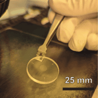
The team’s hybrid meta-atoms are made of a titania-covered resin that is moulded onto the surface of glass substrates of various size as shown in the figure “On display”. The meta-atoms are 900 nm tall, 380 nm long, and 70 nm wide. The titania coating is only 23 nm thick. This type of high-resolution nanopatterning is traditionally expensive and can only be used to cover small areas at one time.
Silicon technology meets nanostamping
Now, Rho and colleagues have simplified the production of metalenses by integrating three already mature fabrication technologies. These are photolithography, nanoimprint lithography and atomic layer deposition. Photolithography involves using deep-ultraviolet lasers to create patterns on silicon wafers. This is a standard technique in the electronics industry and it can also be used to make small-scale metalenses. However, it is an expensive process that is not viable for the large-scale manufacturing of metalenses.
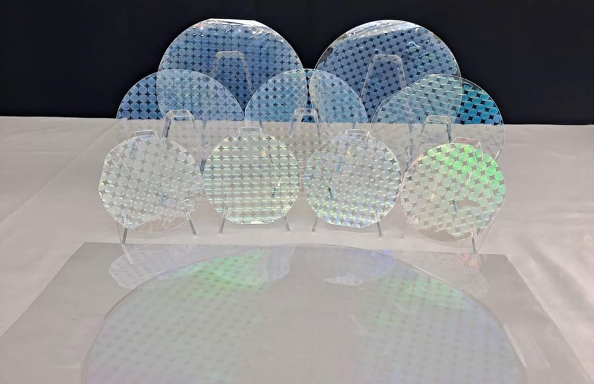
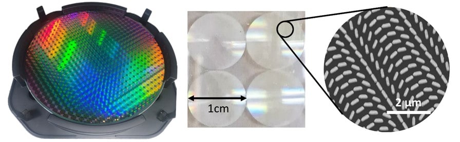
Instead of using deep ultraviolet photolithography to make the metalenses, it was used by the team to pattern a master stamp that was 12 inches (30 cm) across and had a feature resolution of 40 nm (see figure “Production process”). The stamp was used to imprint the inverse of the meta-atom structure in a replica mould made of soft silicone. Liquid resin was then poured into the silicone mould, where it flowed into the nanogrooves before hardening. This allowed the team to make hundreds of metalenses (the 1 cm cylinders in figure 2) at the same time. Indeed, the sophisticated surface structures shown in the scanning electron microscope image (see figure “Production process”) can be made in less than 15 minutes.

The refractive index of the resin is too low to provide the desired control of light, so a thin layer of titania was deposited on top of the resin to increase the index of refraction as well as to boost the mechanical strength of the structure.
Let there be light VR
To demonstrate the potential of the metalenses, the team integrated them in a prototype VR display. Commercial VR devices use reflection or diffraction to project virtual images to the eyes of the user – and this results in bulky devices that must accommodate the appropriate focal length for the optics. Their metalens-based VR display reduces the distance the light has to travel by using a transmission-based design. This makes the display lightweight and comfortable to wear. Although the team only tested the display with static images, the device showed promise by creating images using red, green and blue light; the building blocks of all-colour displays (see figure “Prototype display”).
The researchers say that their scalable fabrication method produces metalenses with higher performance than devices made using more traditional methods. While there is still a lot of room for progress, the advent of mass-produced metalenses opens the door for their use in biosensors, colour printing and holograms – as well as VR displays.