

Fancy some more? Check out our puzzles page.
Back to the Moon: inside the Artemis II mission
More than half a century after the final Apollo mission, humans are returning to the Moon. The latest episode of Physics World Stories reflects on Artemis II – the April 2026 mission that flew four astronauts around the Moon, travelling further from Earth than anyone before them.
The mission marks a major step towards returning humans to the lunar surface and paving the way for a future mission to Mars. It also marked an important societal milestone, as the crew included the first woman, the first person of colour, and the first non-US citizen to fly to the Moon.
Ambre Trujillo of the Planetary Society discusses the excitement surrounding humanity’s return to lunar exploration. In conversation with host Andrew Glester, Trujillo reflects on witnessing her first rocket launch and explains why she sees the Artemis programme as every bit as significant as Apollo for a new generation. Looking ahead, Artemis III in 2027 will test the rendezvous and docking capabilities needed between Orion and commercial landing systems, before Artemis IV aims to return humans to the lunar surface in 2028.
Targeting greener spaceflight
The episode also examines the environmental impact of spaceflight with Alexis Normand, whose company Greenly specializes in carbon accounting. Normand argues that while the space industry’s overall footprint remains relatively small, its ambition and global visibility give it enormous power to inspire wider technological change. Liquid hydrogen was critical in powering Orion’s liftoff and later thrusting it towards the Moon, and could one day help transform aviation into a low-carbon industry. But that hinges hydrogen production itself becoming greener through renewable-powered electrolysis and broader electrification.

Blending lunar ambition with climate innovation, the episode explores how missions to the Moon could help shape the future both in space and here on Earth.
- Find out more about the Artemis II mission in this Physics World feature by science writer and astronomer Keith Cooper
Entangled photons open up potential applications of anti-scattering optics
Engineering light transmission through opaque media is possible thanks to the development of a classical wavefront shaping technique first reported in 2007. Researchers have now demonstrated a quantum entanglement-based method that enables selective image transmission through complex disordered materials.
“We discovered that there might be a way to use quantum properties of light to actually help or improve the problem of imaging through scattering media,” explains Hugo Defienne, a quantum optics researcher at the Paris Institute of Nanosciences (CNRS/Sorbonne University).
In two new research papers, Defienne and his colleagues show how to leverage quantum correlations to engineer incoming light to overcome the scrambling that occurs when it passes through “opaque” scattering materials. The approach could point towards alternatives to the solution pursued so far for unscrambling such light – and could even provide a route towards secure communications, by rendering channels transparent to entangled photon pairs, while remaining opaque to a classical light.
“These works offer a particularly elegant perspective, showing that for spatially entangled photons, the space of wavefront corrections that can compensate scattering is significantly larger than in the classical case,” comments Yaron Bromberg, head of the Complex Photonics Lab at the Hebrew University of Jerusalem in Israel.
Quantum opportunities
In 2007, Allard Mosk and Ivo Vellekoop, both then at the University of Twente in the Netherlands, reported how measurements of the intensity spatial distribution of light distorted by transmission through an opaque scattering material could be used to control the propagation of light and refocus it at the output, effectively turning the scattering material into a lens.
Building on this, in 2010 Sébastien Popoff and Sylvain Gigan showed that they could identify a transformation matrix between the original beams and the transmitted beams, such that applying the inverse to the initial wavefront using a spatial light modulator would allow the original beams to emerge undistorted. Later developments have applied the technique to quantum light. However, being based on intensities of the transmitted light alone, these have not actually exploited light’s quantum properties.
Defienne was working on both the quantum properties of light and the challenge of unscrambling scattered light signals when he began to mull over how to leverage quantum properties in this feedback approach. “We discovered that when you use quantum light, there are many ways of actually unscrambling the light that do not exist when you use a classical system,” he tells Physics World.
Correlation correction
To understand how solutions to the problem multiply for the quantum scenario, it helps to consider a certain type of quantum entanglement that leads to spatially correlated photons. Measure the end point of a photon that’s spatially correlated with another, and the end point of its partner photon will be dictated by the correlation. While scattering media also scramble spatial correlations, a spatial modulator can also invert the scrambling process to retrieve the original spatial correlations.
The quantum bonus comes because whereas with classical light the scattering medium only appears transparent when a one-to-one correspondence between incoming beam and output beam is achieved, there are additional solutions that return an apparently identical spatial correlation distribution between incoming and output entangled photons.
Defienne and his colleagues report the derivations for the quantum approach in Optica. They also demonstrate the approach using a single photon avalanche diode to detect the quantum correlations of light transmitted through a film of paraffin, before feeding it back into a spatial light modulator that adjusts phases to manipulate spatial correlations.
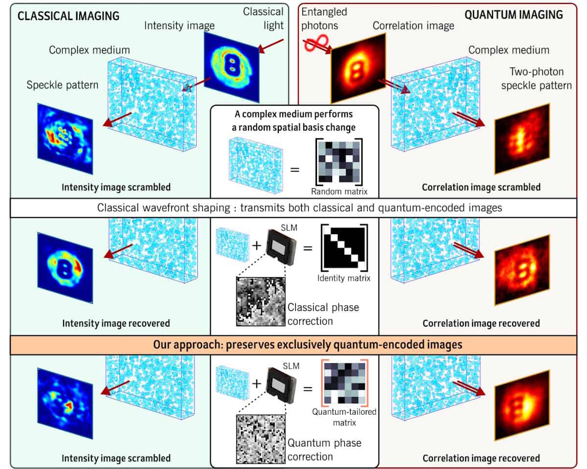
“Conceptually, it’s exactly the same idea,” says Defienne. Nonetheless, almost 20 years on from Mosk and Vellekoop reporting their approach for unscrambling light, this is the first time it has been successfully applied to the quantum properties of light. “It’s just very complex,” Defienne adds. The weak photon pair source, scattering losses in the medium and imperfect detection all pose challenges, such that it can take a long time to have enough data for the required statistics.
“In fact, this is only possible because now we have single-avalanche diode cameras,” says Defienne, noting that these became available with the required sensitivity and frame rate about five years ago. “With any previous camera technology, this is totally impossible.”
Leveraging the quantum properties in this way means that the spatial light modulator unscrambles the quantum correlations while leaving the classical beam still scrambled. The researchers suggest this could serve as a quantum filter that might be useful for blocking nefarious signals intended to muddle transmitted data – by encoding data in quantum correlations it’s possible to block fake data, so long as it is classically encoded. They demonstrate this filtering process in their Nature Physics paper.
Researchers exploit quantum entanglement to create hidden images
Read more

“These results mark a significant breakthrough achieved in experimental samples,” says Sushil Mujumdar from the Tata Institute of Fundamental Research in India, who was not directly involved in the current research. Mujumdar has been working on optimizing wavefront shaping algorithms for quantum light, in particular where the incoming photon count is low. He adds: “The logical segue to this work would be the application of these techniques to thicker and realistic media, which, as acknowledged in the paper, become challenging because of drastically low signal photons, characteristic of the quantum domain.”
Indeed, Defienne and his colleagues are already looking into “some new shaping approach that could be better” for quantum correlated photons passing through, for example, a layer of paint instead of paraffin. They are also looking at the potential to leverage the optical nonlinearity of entangled photon optics for quantum reservoir computing.
Building a better laser on the Moon
There are craters on the Moon where the Sun never shines – and researchers in the US and Germany have shown that these shady locations would be ideal for housing lasers that are more stable than similar devices operated on Earth.
Writing in the Proceedings of the National Academy of Science, Jun Ye at NIST and the University of Colorado and colleagues explain the benefits of installing a silicon optical cavity in a permanently shaded crater. Such a cavity is a block of silicon with internally facing mirrors at opposing ends. Light from a commercial laser is shone into the cavity where it bounces back and forth, growing in intensity and coherence. The length of the cavity defines the frequency of the trapped light. So if the cavity is machined to a very high precision, then the cavity light has a very narrow frequency range.
Some of this light is extracted from the cavity, creating a source of high-quality laser light. To ensure the stability of the laser, the cavity can be cooled to cryogenic temperatures to minimize thermal fluctuations. Now, Ye and colleagues have shown that this stability can be improved significantly if a cavity is operated in a shady nook on the Moon.
Cold vacuum
There are more than 300 regions of the Moon that are in permanent shadow. As well as being enveloped in darkness, these regions tend to maintain a steady temperature of about 50 K. While the Moon has no real atmosphere, it is not surrounded by a perfect vacuum. Radioactive decay and bombardment by meteorites, the solar wind and sunlight liberates molecules from the surface and these will linger briefly before escaping into space. Because dark craters are not subject to bombardment, there should be fewer gas molecules in these regions – and therefore a better vacuum than on the surface. Indeed, the team calculates that pressures of less than 10−10 Pa should exist in these craters, which is well within the ultrahigh vacuum regime.
As a result, dark craters should be a perfect environment for operating a silicon optical cavity. There it would experience a small number of collisions with gas molecules, boosting its stability. What is more, by radiating heat out of the crater and into space, Ye and colleagues reckon that an optical cavity could be further cooled to a chilly 16 K. At this temperature, silicon will neither expand nor contract in response to tiny temperature fluctuations – further stabilizing the output of the cavity.
According to the researchers’ modelling, such a cavity would have a very low thermal noise-limited stability of 10−18 and a coherence time exceeding 1 min. This performance, they say, is ten times better than that achieved by the best cavities operated on Earth.
Testing Einstein
The team proposes several different uses for light emitted by the cavity. Because it would have a very stable frequency, it could be used as a very precise lunar time signal. This would be very useful for the navigation on, or near to, the Moon as well as for scientific experiments – including those that test Einstein’s general theory of relatively.
Ultrastable lasers would also allow scientists to create long-baseline interferometers for astronomical observations, including the detection of gravitational waves. Furthermore, the cavities themselves could also be used as detectors. Gravitational waves at certain frequencies would affect the output of a cavity – as could hypothetical interactions between silicon atoms and dark matter.
Using a high-powered relay laser, the cavity signal could be transmitted to lunar satellites that contain atomic clocks – creating a timing network similar to Earth’s global navigation satellite systems such as GPS. Furthermore, light from the cavity could be used to create a quantum network that stretches from the Moon to the Earth.
Team member Yiqi Ni works for the US-based company Lunetronic, which is developing technologies for use in permanently shadowed craters. Ni says that a silicon optical cavity could be operated in low-Earth orbit within two years – and be installed on the Moon within three to five years.
The team also includes researchers from the US National Institute for Standards and Technology (NIST) and PTB, which is Germany’s national metrology and standards institute.
Word wave puzzle no.4
Here’s how the game works:
-
- Enter a word guess – in this game the word has six letters.
- After submitting your guess, each letter in the guessed word is coloured to provide feedback:
- Green: The letter is correct and is in the correct position in the target word.
- Yellow: The letter is correct but is in the wrong position in the target word.
- Grey: The letter is not in the target word at all.
- Using this colour feedback, refine your next guess.
- Continue guessing until you correctly identify the hidden word(s) or run out of attempts.
If you need any hints, read the article here.
Fancy some more? Check out our puzzles page.
Thermodynamic computing: noise as a resource, not an enemy
Noise is the enemy of many computing paradigms. Conventional computers are power hungry because they must operate at energy levels well above those of electronic fluctuations in silicon. The problem is much more acute in quantum computing, where noise is a significant barrier to creating practical processors.
But what if we could use noise as a computational resource? That is the idea behind thermodynamic computing – which is the focus of this episode of the Physics World Weekly podcast. My guest is the theoretical physicist Stephen Whitelam – who joins me down the line from Lawrence Berkeley National Laboratory in the US.
- “Generative Thermodynamic Computing” by Stephen Whitelam
Particle size affects contact electrification
Static electricity is an everyday phenomenon, but it is not well understood. Researchers at the University of Chile have now added another piece to the puzzle by conducting experiments on the charge distributions of free-falling particles. They found that same-sized particles within the sample had the same range of surface charge densities, suggesting that particle size plays a major role in static electricity. Their work could improve our understanding of how charge behaves on insulating surfaces, with implications in areas ranging from planet formation to lightning generation in volcanic plumes and clogging in industrial processes.
Static electricity is also known as contact electrification because it occurs when charge transfers from one object to another as the two touch each other. (Think of rubbing a balloon on someone’s head to make their hair stand on end). The phenomenon is present in many situations, including pollen transport, grinding coffee, and ash particles in volcanic plumes, which can generate lightning. Electrostatic charging also creates strong electric fields in sandstorms on Earth and dust storms both here and on Mars. Charged dust could even be involved in the formation of rocky planets.
To understand and model the effects of electrostatic charging, researchers need to find out how particles become charged and, once that happens, how these charges are distributed. “In an ideal experiment, we could study a large ensemble of same-material, initially neutral grains,” says Nicolás Mujica, the physicist who led the study. “After many contacts and collisions between the grains, we should observe a stationary and stable charge probability distribution function that has both positive and negative charges.”
Researchers have previously observed this effect by imaging the trajectories of particles in free fall as an electric field was applied to them in microgravity conditions. The charge probability distribution functions (PDFs) measured in these experiments are generally non-Gaussian, with “fat” tails that may point to the existence of memory effects in the charge exchange process between the particles. “It is much more likely to have highly charged particles in an ensemble that what we would naively expect,” Mujica says.
Free-fall videography technique
Mujica and colleagues measured the charge distributions of ZrO2:SiO2 composite particles using a free-fall videography technique they developed in a previous study. The particles ranged from 172 to 545 μm in diameter and each sample focused on a single size. As well as buying the particles from the same vendor to ensure they were as identical as possible, the team further characterized them using x-ray fluorescence (XRF) and atomic force microscopy (AFM) to determine their precise chemical composition and surface roughness, respectively.
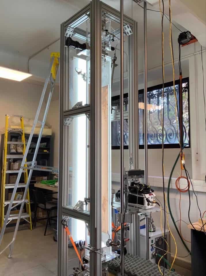
In their experiments, the Chile researchers released the particles from a 3 m drop tower, which is essentially a huge, transparent hourglass structure under vacuum with electrodes on either side that generate a static electric field. Inside this tower, the particles rub against each other during their quasistatic flow and become either positively or negatively charged in the process. The static electric field accelerates these charged particles sideways, and the researchers measure this acceleration by capturing the particles on video as they exit the tower. By combining the particles’ known mass with their measured accelerations, the team can calculate the particles’ charges.
Next, Mujica and colleagues plotted the probability that a certain amount of charge would be found on a given particle. Since charges could be either positive or negative, all the PDFs, regardless of particle size, resembled non-Gaussian curves with peaks at zero charge. However, the widths of these curves varied systematically with the surface areas of the particles. According to the researchers, this result indicates that the charging of the particles depends on the particles’ size.
Towards a microscopic model of charge exchange
The researchers say their study began with a simple question: how do planets form? “There are some important missing pieces in this big puzzle and one of them is the effect of electric charges,” Mujica says. The team’s results, he says, are evidence that charge can indeed help particle clusters to form in space.
Their main challenge, he recalls, was constructing the drop tower. The first prototype did not work because of a fundamental design problem, and while the second worked better, it broke after a few years because of the forces (about 40 kN) exerted on each side of the chamber due to the vacuum within. “The third and current version is working fine and we expect it to live long enough to take more useful data,” Mujica says.
The researchers, who report their work in Physical Review Materials, say their next step will be to develop a microscopic model of charge exchange from which they can determine the measured charge distributions. “We will then adapt this model for mixtures of particles, either of different sizes or materials, and try to simulate more realistic situations, comparing the predictions with measurements,” says Mujica.
“It has also been recently demonstrated that adventitious carbon, a thin, ubiquitous layer of carbonaceous contamination (typically a few nm thick) that forms on most surfaces exposed to air, plays a big role in the way oxide particles exchange charge,” he adds. “We therefore intend to study the charge segregation that usually occurs between large and small grains and the effect of surface cleaning processes.”
Multiplexed MRI expands the power of conventional brain imaging
MRI is a powerful diagnostic imaging tool, with more than 100 million scans performed worldwide each year. While MR signals contain rich information from multiple molecules and numerous physical and biological processes, current clinical MRI exams rely solely on signals from water molecules in tissues and generally only obtain one tissue biomarker at a time. But MRI could do so much more.
A research team headed up at the University of Illinois Urbana-Champaign has done just that, devising a new MRI technique – multiplexed MRI (MRx) – that enables simultaneous mapping of multiple molecular signals using a standard clinical 3 T MRI scanner.
The barrier to performing multiparametric imaging with conventional MRI lies in the “curse of dimensionality”, in which high-dimensional imaging requires prohibitively long scan times. Multimolecular MRI, meanwhile, is limited by weak signals from brain metabolites and neurotransmitters (typically 1000–10,000 times weaker than proton-based signals from water molecules), which often overlap, making them difficult to detect and separate.
“MRx overcomes these challenges through specialized data acquisition and processing strategies,” explains study leader Zhi-Pei Liang. “During data acquisition, MRx simultaneously excites and encodes all detectable molecular signals with sparse sampling to achieve high imaging speed. During data processing, MRx employs physics-driven machine learning methods to separate and quantify the different signal components.”
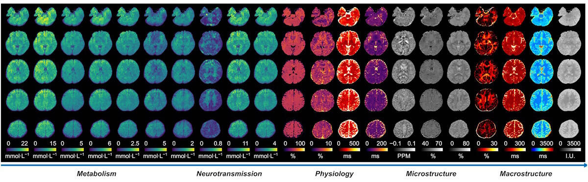
Reporting their findings in Nature, the researchers demonstrate high-resolution mapping of 22 quantitative biomarkers of the whole brain in a single scan. They also show how a new sparse sampling scheme enables acquisition of these biomarkers in just 14 min – significantly shorter than clinical multi-contrast MRI protocols that can take up to an hour.
“Our main motivation was to develop an ‘omni’ imaging technology that fully harnesses the rich biological information embedded in magnetic resonance signals, enabling us to unravel the structural, physiological and molecular fingerprints of brain function and diseases,” says Liang.
In vivo studies
MRI is widely used within brain tumour diagnosis to evaluate tumour location, size and extent, and blood–brain barrier disruption. However, standard MRI scans do not directly reveal the underlying pathophysiological changes and tumour heterogeneity. MRx, on the other hand, can acquire a wide range of biomarkers that provide valuable information on processes such as neuronal loss, energy metabolism, axonal damage, hypoxia, demyelination and many more.
To test the technique, Liang and colleagues performed MRx imaging on patients with clinically diagnosed brain tumours, using machine learning to combine the measured biomarkers into a single variable defining the tissue state at each pixel. This MRx “tissue state index” could differentiate eight distinct tissue states: grey matter; white matter; cerebrospinal fluid; oedema (fluid build-up); meningioma; low and high-grade oligodendroglioma; and glioblastoma. Standard multiparametric MRI failed to separate these states.
This ability to accurately characterize tissue states could enable a range of essential clinical tasks, such as grading low- versus high-grade brain tumours, for example, or separating glioblastoma from oedema during radiation therapy planning.
MRx could also prove invaluable for lesion characterization in multiple sclerosis (MS), a critical process for stratifying patients, planning treatment and predicting disease progression. The researchers demonstrated that MRx of patients with MS could differentiate active and chronic MS lesions without requiring contrast agents (as in current practice), attributed to the technique’s ability to visualize biomarkers specific to individual pathophysiological processes.
Such MRx biomarkers also helped to predict lesion progression, by capturing key pathophysiological features that cannot be revealed by conventional MRI, a feature that could enable early interventions and improve patient outcome.
Beyond cancer and MS, many other brain diseases could also benefit from MRx, including stroke, epilepsy and Alzheimer’s disease, for example. “MRx is expected to open up new opportunities for brain mapping and for precision healthcare of brain diseases, including neurological and neurodegenerative disorders,” says Liang.
For the proton-based studies reported in this latest study, MRx was performed without needing any modifications to the MRI scanner hardware. Instead, the method is implemented using a new pulse sequence for data acquisition plus custom software for data processing. Liang notes that extending MRx to include multiple nuclei – such as sodium, phosphorus, and deuterium – will require specialized multinuclear RF coil hardware.
“Our current efforts are focused on further improving the robustness and reliability of MRx under practical clinical imaging conditions, to facilitate both scientific studies and clinical translation,” he tells Physics World, noting that MRx has already been licensed (through Siemens) to imaging centres worldwide for evaluation of its clinical potential. “We are also expanding the technology to map additional molecular species and, ultimately, to enable multinuclear multiplexed imaging beyond protons.”
Thyracont’s vacuum measurement instruments enable innovation across industries
Life sciences: reliable conditions for pharmaceutical freeze drying
Freeze drying (lyophilization) plays an important role in the manufacture of pharmaceuticals extending shelf life by removing water via sublimation under vacuum conditions. Because these processes run over long cycles, stable and contamination-resistant vacuum measurement is essential.
Thyracont’s VCP transducer is designed for such applications. Its platinum-rhodium filament provides high resistance against corrosion and contamination, supports sterilization and reliable operation under thermal stress. Operating in the fine vacuum range (1000 to 5 × 10−⁴ mbar), it ensures stable process control in freeze-drying systems.
“Long-term stability and resistance against corrosive process media are decisive factors in freeze-drying processes. The VCP was specifically engineered to maintain reliable performance even withstanding steam sterilizations,” explains Frank P Salzberger, CEO of Thyracont.
High-tech and research: enabling analytical precision
Many of the cutting-edge instruments used in analytics and R&D operate under vacuum – including those used for mass spectrometry and materials testing. In applications such as beverage gas analysis, the VSP63MV Pirani transducer enables precise monitoring in the 1000 to 10−4 mbar range, supporting zero adjustment of the mass spectrometer, which is essential for the reliable detection of trace contaminants at very low concentrations.
The analysis of the thermomechanical properties of materials is necessary for the development of cryogenic technologies including those used in quantum technologies. This involves cooling materials and devices to very low temperatures and measuring how their physical properties change. Thyracont vacuum gauges such as the VSP63DL and VSM77D cover fine and high vacuum ranges down to ultra-high vacuum conditions, enabling stable thermomechanical characterization of materials at extreme temperatures.
Semiconductor and coating processes: stability in complex systems
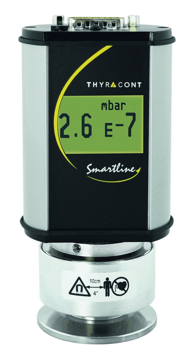
In semiconductor manufacturing, wafer bonding requires tightly controlled vacuum conditions to ensure contamination-free and uniform layer formation. During initial evacuation, Thyracont’s VSC43MA4 is used to monitor roughing and bypass pumping stages.
In subsequent high-vacuum stages, Smartline VSM transducers provide reliable measurement from atmospheric pressure to ultra-high vacuum, combining Pirani and cold cathode technologies with optimized range switching for stable operation.
“In semiconductor wafer bonding, it is essential to maintain stable measurement across the full pressure range – from roughing to ultra-high vacuum. Our Smartline VSM series ensures exactly this seamless transition,” says Salzberger.
In optical coating applications, this approach ensures continuous monitoring while protecting sensitive sensor components.
Industrial vacuum processes: distillation and thermal treatment
Short-path distillation relies on precise vacuum control (typically 1 × 10−³ to 1 mbar) to enable gentle separation of heat-sensitive substances such as fragrances. A thin film is formed inside the chamber, and evaporation occurs at reduced temperatures, preserving delicate compounds.
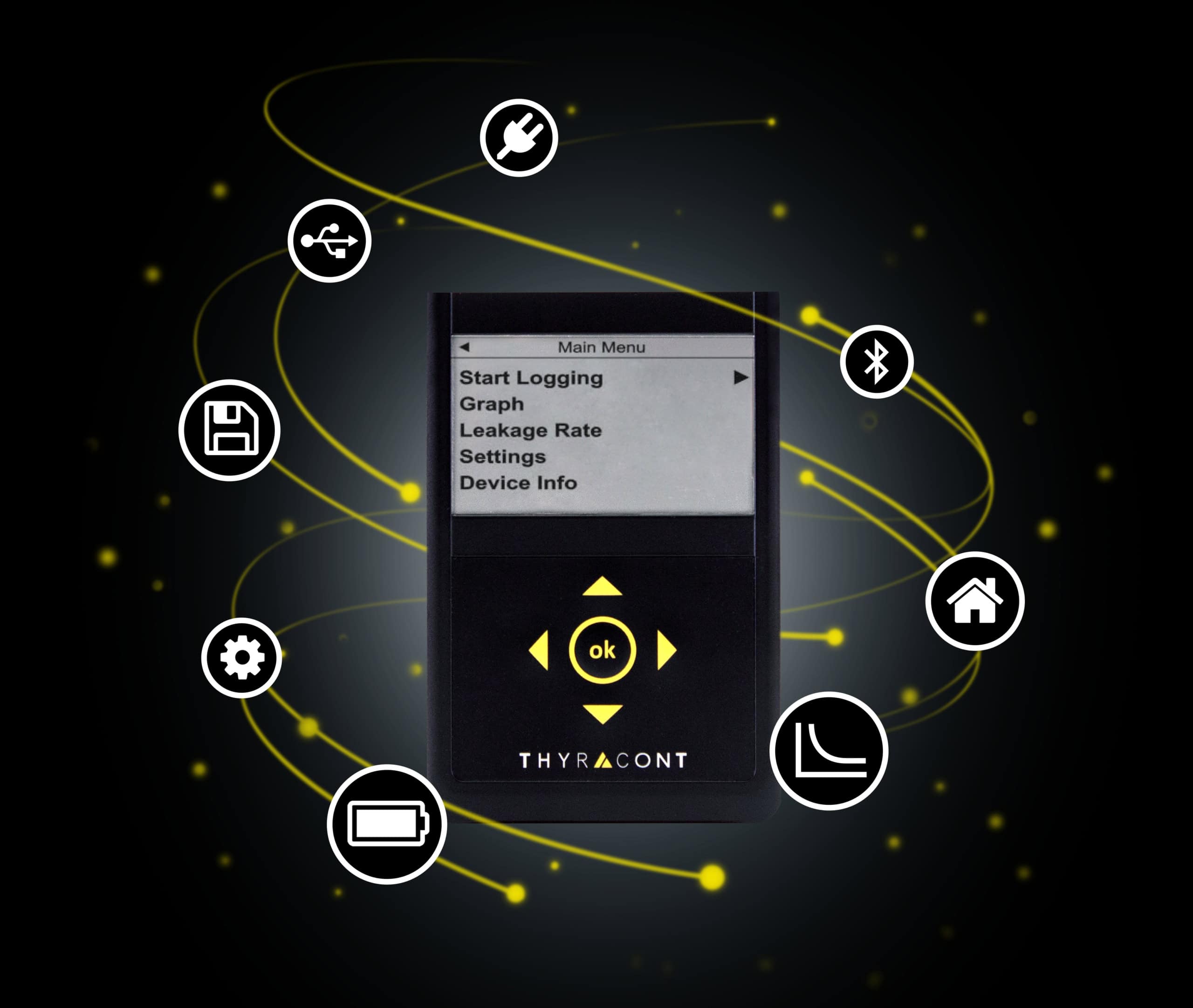
Stable pressure control is essential to ensure consistent product quality. Devices such as the VD64P and VD850 support monitoring and control functions including switching outputs, leak detection, and integrated data logging for process documentation.
Peter Gerlesberger, development manager at Thyracont explains, “Reliable leak testing ensures that vacuum chambers and systems meet the required process conditions. With the VD850 users can quickly and reliably determine the magnitude of the leak rate”.
Vacuum furnaces face similar requirements under high-temperature and contamination conditions. The VD850, as well as VSH transducers (Pirani/hot cathode), enable reliable pressure measurement across furnace inlet and outlet zones.
Packaging applications: quality control in food safety
Vacuum packaging plays a crucial role in in the food industry, extending shelf life and reducing food waste. Ensuring consistent vacuum levels is critical for product safety and quality.
Testing is performed by replacing the food with a vacuum gauge and monitoring the pressure after sealing. The compact VD810 can be temporarily integrated directly into packaging, thereby simulating real-world process conditions.
The built-in piezo-ceramic sensor measures absolute and relative pressure in a rough vacuum and records pressure curves with timestamps. The recorded measurement data can be downloaded via USB or, optionally, via Bluetooth LE and used for process analysis and quality documentation.
The common thread
Across industries, from life sciences to semiconductor manufacturing, Thyracont vacuum measurement technology enables precise, stable, and reliable process control under demanding conditions. By combining robust sensor design with wide measurement ranges and intelligent system integration, these instruments contribute to the performance and quality of modern industrial and research applications.
Electron beams rearrange atoms in a 3D crystal
Ultra-precise electron beams can rearrange atoms in a 3D crystal lattice and create structures not found in nature, an international team of researchers has shown. The work could have implications for quantum simulation and atomic-scale manufacturing.
The 1986 Nobel Prize for Physics was divided between three researchers. Half was split between Gerd Binnig and Heinrich Rohrer of IBM’s Zurich laboratory for their development of the scanning tunnelling microscope (STM). The STM’s ability not just to image but to move atoms was famously demonstrated three years later, when Don Eigler and Erhard Schweizer of IBM Almaden in California produced a picture of 35 xenon atoms precisely placed on a crystal of nickel to spell out the letters “IBM”. STMs have become widely used in surface analysis. However, they can only manipulate 2D surfaces, are painstakingly slow and require high vacuum and ultracold temperatures.
The other half of the 1986 prize went to Ernst Ruska of Germany’s Max Planck Society for his invention of the electron microscope – which can image samples with atomic resolution. Until now, however, electron microscopes had not been able to deterministically manipulate atoms because their high-energy electron beams tend to break bonds randomly within a crystal.
Now researchers in the group of Frances Ross at Massachusetts Institute of Technology led by Julian Klein, together with Kevin Roccapriore of Oak Ridge National Laboratory and others, used Oak Ridge’s ultra-precise, extremely stable, focused electron beam to penetrate around 13 nm into a crystal of the layered van der Waals material chromium sulphide bromide.
Interesting crystal structure
“The material has a very interesting crystal structure,” says Klein; “One individual layer has a mixture of sulphur and chromium atoms, but then on both sides of this layer there are bromine atoms sticking out in both directions. And when you stack those crystals you create atom-sized gaps between the layers.”
When the electron beam is positioned within 20 pm of its target and then moved slightly in a specific direction, the electrons in the beam can nudge the chromium atoms in the line of fire out of their original positions into the target unoccupied sites. This creates lattice defects called vacancy–interstitial complexes. Computer simulations suggest that, owing to interlayer interactions, movement of the chromium atom in one layer should encourage the transformation of layers above or below. Ross says that “[the transformed layers] do form in a timed sequence, but we can’t tell in what order they’re transforming”.
By carefully manipulating the electron beam across the surface of the crystal, the researchers can create an array of vacancy–interstitial complexes: “Julian and Kevin have a series of images at different times,” says Ross; “You can see the quality of the result just gets better and better…The beam has to be exactly on that column of atoms because otherwise some of the energy is going to go into the wrong place and disrupt the rest of the lattice.”
More robust crystals
The resulting 3D crystal is much more robust than an STM-created surface. “The defects created in the interior of the crystal are protected from the environment,” Ross explains. This allows measurements of different properties in different laboratories without needing cryogenic refrigeration or vacuum.
This could also ease the path to practical application for what is, say the researchers, an emergent many-body state. “That’s where the fun stuff comes in,” Ross says. “I’m excited because of the scalability of this that allows us to look at the interactions between the defects rather than just creating a defect itself. The stability of the microscopes that allows us to keep going and create a huge array is really exciting.” The researchers are examining various possible applications in, for example, quantum simulation and the manufacturing of matter with atomic-scale precision.
The team describes its work in Nature.
“It’s a fascinating paper,” says materials scientist and STM expert Ludwig Bartels of the University of California, Riverside. “It’s definitely above the scale of what scanning tunnelling microscopy could do…and, as they discussed in their paper, it’s probably a really interesting scale in which they can think about electronic states extending between the different defects they are making.”
He says that, while he does not believe this will ever be the way computer chips are made “it is definitely an order of magnitude above what was possible before”. Moreover, he says that the ideas used in the paper to monitor the motion of the atoms remind him of those developed 30 years ago for STM. “They are not exactly the same, but they are reminiscent, and they are just as ingenious,” he says.
Copyright © 2026 by IOP Publishing Ltd and individual contributors