Applying a magnetic field to graphene superlattices produces room temperature quantum oscillations created by delocalized quasiparticles known as magnetic Bloch states. These states should be generic to any superlattice system, not just graphene, and the new finding will be important for fundamental electron transport studies. It will also be crucial for characterizing and understanding novel superlattice devices based on 2D materials like graphene.
“Our study proves that it is possible to create new metallic systems within the same material by applying a magnetic field,” explains team member Roshan Krishna Kumar of the University of Manchester, UK. “These new metals have unique properties compared to those to which no magnetic field is applied, thus providing a new playground for studying condensed matter physics.”
New class of metallic system
The new result comes hot on the heels of work done last year, in which the researchers, led by Sir Andre Geim, observed robust (Brown-Zak) quantum oscillations in the magneto-conductivity of graphene (a sheet of carbon just one atom thick) at certain values of magnetic field. This study, published in Science DOI: 10.1126/science.aal3357, showed that these magnetic Bloch states, could be observed well above room temperature. The new work, detailed in PNAS this time, reveals high-order magnetic Bloch states that represent a new class of metallic system.
“Usually such experiments are done at liquid helium temperatures (around 4 K) to reduce lattice vibrations and study quantized phenomena,” says Krishna Kumar. “The data obtained can be rather difficult to interpret, however, because there can be multiple effects happening all at once. In graphene superlattices, for example, Brown-Zak and Shubnikov-de Haas oscillations co-exist at low temperatures. Our new approach involves heating samples to 100-200 K. This ‘smears’ most of the quantized effects so that our measurements only capture the behaviour of magnetic Bloch states.”
Fractal pattern in the magneto-conductivity
As reported in the PNAS paper, these states are present in second-, third-, and fourth-orders, and this full hierarchy creates a fascinating fractal pattern in the magneto-conductivity, Krishna Kumar tells nanotechweb.org. The pattern is intimately related to the way Hofstadter butterflies (striking fractal patterns that describe the behaviour of electrons in a magnetic field) originate. This complete fractal structure can indeed only appear due to high-order magnetic Bloch states and had never been seen in a graphene superlattice experiment until now.
A Bloch state is the quantum mechanical description of an electron in a solid-state crystal. It explains one of the puzzling questions in condensed matter physics: how can a negatively charged electron move through the crystal without bumping into the positively-charged cores?
Electrons carry on moving as if there were no field
“If we apply a strong magnetic field perpendicular to the crystal, we destroy this Bloch state because electrons experience the Lorentz force and become ‘stuck’ on closed orbits,” explains Krishna Kumar. “In our experiments, we show that electrons can move freely as a Bloch state under a certain applied magnetic field (one whose ‘magnetic length’ is commensurable with the periodicity of the superlattice). In other words, the electrons carry on moving as if there were no field applied.”
Mathematically, this effect occurs each time an integer number of magnetic flux quanta (φ) pierce an integer number of crystal unit cells, according to φ = SB = φ0p/q, where S is the area of a crystal’s unit cell and p and q are integer numbers. “It is impossible to find such magnetic Bloch states in typical crystals because we would require unfeasibly high magnetic fields (of 10 000 Tesla) to see them, says Krishna Kumar. However, the beauty of graphene superlattices is that they are significantly larger than naturally occurring crystals (50 times larger in our case). In these systems, we only have to apply field of around 4 Tesla to observe the magnetic Bloch states, which is relatively easy with the magnets available today.
Any superlattice
We should be able to observe these Bloch states in any superlattice, not just graphene, he adds. “Our findings will be important for electron transport studies, since the physics involved is one of the most fundamental aspects of magneto-transport in solid state-crystals. Our work will thus help us better characterize and understand novel devices based on 2D superlattice materials.
“These states are essentially a new class of material with different properties compared to ordinary graphene. For example, many of the first-order magnetic Bloch states host pronounced band gaps, in contrast to graphene, which is a zero-gapped semi-metal. Now that we have identified higher-order states, our next step will be to understand exactly how they behave.
Like many 2D materials, gallium sports some fascinating properties when in the form of atom thick layers. It has a superconducting transition temperature at 5.4 K and interesting superconductor-metal transitions with increasing magnetic field. In addition, like bulk gallium, which is widely used in electronics in III-V semiconductor compounds, 2D gallenene may also be useful in optoelectronic devices. In a recent 2D Materials report, Jun-Zhong Wang and colleagues at the School of Physical Science and Technology Southwest University in China show how to grow gallenene epitaxially on the (1 1 1) plane of silicon, helping towards the possible incorporation of gallenene in future electronic and optoelectronic devices.
Despite the success of epitaxial growth to produce graphene and other 2D materials, with its low melting temperature growing 2D gallium has presented difficulties. As Wang and colleagues point out the 7 × 7 (1 1 1) plane of silicon – the crystal orientation of the wafers commonly used for silicon electronics – has dangling bonds that interact strongly with gallium atoms and inhibit their migration along the surface.
Previous work by researchers at Rice University and Hysitron Inc in the US reported gallenene production by exfoliating from molten gallium but Wang and colleagues have shown that it is possible to epitaxially grow gallenene on silicon.
Layered success
The researchers deposit a third of a monolayer of gallium on the Si(1 1 1) − 7 × 7 surface at room temperature and anneal it at 550 °C for 30 min to produce a layer of √3 × √3 gallium. They then grow a buffer layer at 50 °C using a beam of gallium at a flux of 0.2 monolayers per minute. On this buffer layer they could readily grow honeycomb 2D gallanene.
They use scanning tunnelling microscopy alongside first principal calculations to derive the structure of the layers, identifying a 4 × √13 structure for the buffer layer. They also confirm the metallic behaviour of the gallenene top layer.
“As we all know, silicon is the backbone of the traditional semiconductor industry,” explain Wang and colleagues in their report. “If gallenene can be synthesized on the surface of silicon, its potential applications in optoelectronic and microelectronic devices will be greatly improved.”
Bone is certainly an impressive natural material because it is both stiff (it endures load without deforming much) and tough (it endures load and deformation without breaking). Stiffness and toughness are rarely found together in materials. The strength of bone comes from two main components: the mineral calcium phosphate (of the apatite variety), and the protein collagen.
The way in which bone collagen and mineral organize themselves has proved difficult to understand, however, because the way they assemble is complex at every length scale. Scanning transmission electron microscopy tomography experiments by researchers led by Roland Kröger of the University of York and Molly Stevens of Imperial College London, both in the UK,have now revealed, among other things, that bone mineral is hierarchically organized from the nanoscale upwards. It is composed of curved needle-like crystallites that merge into twisted plates that form larger aggregates, thus creating a bridge between adjacent collagen fibrils.
The findings could be important for a variety of fields, including osteology and archeology. They will also provide valuable insight into skeletal diseases, growth and development, and might even help in the design of novel biomimetic materials.
Evaluating the mineral phase of bone in 3D
Kröger and Stevens set out to evaluate the mineral phase of bone in 3D. They used electron tomography – that means collecting images at many sequential angles or “tilts” – to reconstruct 3D images of their samples.
One of their observations, for example, was the slight curvature of crystallites across their lengths. Another was stacks of parallel twisted crystallites around irregular voids in the oblique direction. Finally, they saw tight packing of hexagonal crystals into rosette shapes in perpendicular projections. “We developed a model that puts all these observations together that shows that crystals are curved, hierarchical and splaying to form a continuous cross-fibrillar network,” explain Kröger and Stevens.
Fractal-like helical motifs
“The twisting crystals in bone assemble with twisted collagen chains and form fibrils that are twisted themselves”, they add. “As known from earlier studies, the fibrils twist into concentric layers that gently twist themselves around tiny capillaries in bone, which in turn twist around the bone’s long axis, which is often curved into a helix (like a rib, or a collar bone).”
The researchers say that the helical twist is self-similar, or fractal-like. Fractal-like helical motifs are ubiquitous in nature (think of ferns or cauliflower). “This type of organization might have evolved over millions of years to optimize bone structure and function,” lead author of this study Natalie Reznikov tells nanotechweb.org.
Yong Mao of the University of Nottingham in the UK agrees: “This is certainly an interesting study, contributing to the understanding of bone structure,” he comments. “I think researchers are increasingly appreciating the fractal/hierarchical nature of the world, which generally offers an evolutionary advantage. These finer structures are becoming more accessible with the development of additive manufacturing (or 3D printing). I expect this to be an exciting field of development in the future.
Individual meal choices have a profound effect on our environmental footprint, but much of the analysis has been based on aggregated or stereotyped diets. Now researchers have examined the food choices of more than 16,000 US residents on a single day.
The study shows that an environmental saving equivalent to cutting 661 million passenger vehicle miles could occur if just the top 20% of most intensively emitting meals on a given day were replaced with a diet with the average impact – 4.7 kg of carbon dioxide equivalent.
What’s more, these savings soon add up. The group reported that such a hypothetical diet shift – if implemented every day – could bring the US 9.6% closer to achieving UN Framework Convention on Climate Change targets for 2025.
“One of the key outcomes is being able to represent the greenhouse gas emissions and energy impacts associated with the US diet as a distribution across the population,” said Martin Heller of the University of Michigan.
To examine greenhouse gas emissions and energy use meal by meal, Heller and colleagues linked food life cycle assessment studies to the US National Health and Nutrition Examination Survey (NHANES). Featuring over 16,000 responses, the analysis offers a nationally representative snapshot based on self-selected diets across the country over one day.
The linked database reveals some striking differences in food choices and could help to shape future educational campaigns and policy efforts aimed at encouraging diet shift.
The analysis required pairing over 6000 as-consumed foods and dishes with more than 300 life cycle assessment studies. But the challenges didn’t stop there.
“We had to fill in gaps in the literature by making informed proxy assignments,” said Heller. “However, it turns out these proxies have very little effect on the overall results because they tend to be foods that are consumed in low quantities in the US diet and have relatively low impacts.”
So what advice does the team have so far? “The first recommendation is to pay attention to nutritional needs and avoid excess calories as more food equals more impact,” said Heller. “The second is to be mindful of the consumption of animal-based foods.”
The study highlights that even modest reductions in meat and dairy intake can make a big difference in terms of greenhouse gas emissions saved. Adding to this is the issue of food waste.
“NHANES doesn’t have direct data on food losses, but using other data from USDA that we connected to our databases, we estimated that food losses, at both the retail and consumer level, represent about a quarter of impacts from producing the US diet,” said Diego Rose of Tulane University.
The team’s approach opens the door to assessing how diets contribute jointly to both environmental and health outcomes.
“Establishing a framework for linking the environmental impact of foods to individual diets opens up a whole host of research questions, including further exploration into policy options, economic and social justice considerations,” said Heller.
Future plans include expanding the research to factor in other environmental impacts such as water use and land use.
The ESTRO 37 meeting in Barcelona saw Accuray unveil a range of product advancements, including the launch of CTrue IR, an iterative reconstruction algorithm currently available on the Radixact System, which provides image-guided, intensity-modulated radiotherapy.
The Radixact treatment device encompasses integrated 3D volumetric imaging, using low-dose fan-beam CT images for daily set-up and registration. The system also offers Delivery Analysis software that leverages the same integrated detector to perform pre-treatment dose calculations and post-treatment analysis of exit fluence through the patient for every fraction, and generates warnings if any parameters fall outside of clinically acceptable windows.
The new image-guidance software can reconstruct these CT fan-beam scans with enhanced image quality, while maintaining a low imaging dose and the ability to perform live reconstruction as the images are acquired. The main benefit of iterative reconstruction is the much improved signal-to-noise ratio, which in turn increases the soft-tissue contrast.
“Iterative reconstruction reduces the noise by over a factor of two and helps improve image uniformity,” explained Accuray’s Andrea Cox. “It particularly enhances images in the superior-inferior direction, so that the slice transitions are less visible, and improves soft-tissue visibility in all image planes.”
The CTrue IR software is now installed at three customer sites, one in Europe and two in the US, with the first clinical images recorded just a couple of weeks ago. Cox described one of the first clinical test cases that used the new software release – an obese patient with a hip prosthesis.
Such a case could result in a sub-optimal CT scan, due to photon starvation artefacts (which occur due to photon attenuation through obese patients) and metal artefacts arising from the prosthesis. Using the CTrue imaging system with the new iterative reconstruction capability, the image exhibited excellent uniformity, with no problem with artefacts.
“The first customer to use this software found much improved image uniformity,” said Cox. “The therapists are more confident now in the positioning of the patient, they’re really happy with it.”
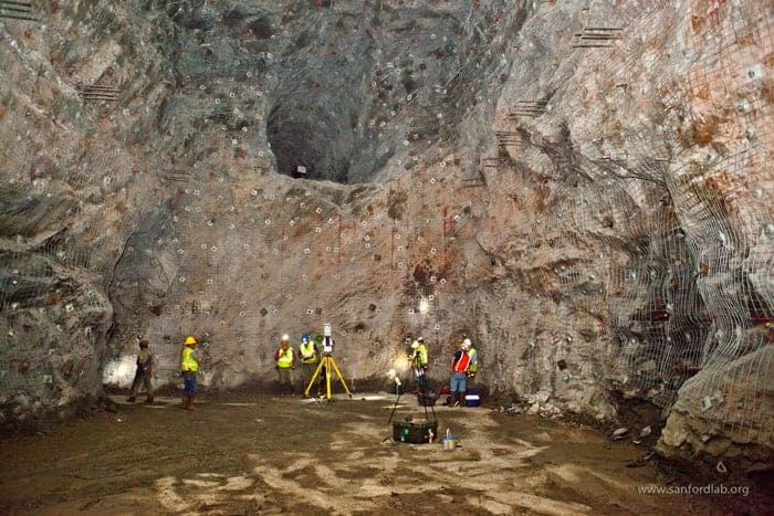
Construction of a new Super Cryogenic Dark Matter Search (SuperCDMS) dark-matter detector can begin now that the next round of funding for the experiment has been has been approved by the US Department of Energy (DOE). The detector should start taking data in the early 2020s and will be located 2 km below the Earth’s surface at SNOLAB in Sudbury, Canada. The experiment will be at least 50 times more sensitive than the previous SuperCDMS experiment, which ran in 2012-13 in the Soudan Underground Laboratory in Minnesota.
The DOE will contribute $19m towards building the detector, while the US National Science Foundation will pay $12m and the Canadian Foundation for Innovation will fork out $3m. The SuperCDMS collaboration involves 111 physicists at 26 institutions in the US, Canada, France and the UK.
The detector will look for weakly interacting massive particles (WIMPs), which are hypothetical dark-matter particles that could account for 85% of the matter in the universe. While indirect evidence for dark matter abounds in astronomical observations, physicists have yet to make a direct detection of the mysterious stuff. Doing so would be a major leap forward in astrophysics and could also point to new physics beyond the Standard Model of particle physics.
Extreme sensitivity
WIMPs are a family of hypothetical dark-matter particles that interact very weakly with ordinary matter. This means that if physicists want to detect WIMPs, they must use an extremely sensitive detector – ideally located deep underground, where it is shielded from cosmic rays and other background radiation.
According to Richard Partridge, head of the SuperCDMS group at the Kavli Institute for Particle Astrophysics and Cosmology at Stanford University, the new experiment will be “the world’s most sensitive for relatively light WIMPs – in a mass range from a fraction of the proton mass to about 10 proton masses”. He calls this sensitivity “unparalleled” and says it will “create exciting opportunities to explore new territory in dark-matter research”.
The SNOLAB experiment will look for WIMPs using silicon and germanium crystals that will be cooled to about 10 mK and surrounded by superconducting aluminium. The hope is that WIMPs will interact with an atomic nucleus in a crystal, creating tiny vibrations (or phonons) that propagate to the edge of the crystal and enter the aluminium. Once in the aluminium, the phonons transfer their energy to superconducting Cooper pairs, causing pairs to break and leading to a large increase in electrical resistance, which can be detected. WIMP-nucleus interactions should also produces electrons and holes in the crystal, which will be detected electronically.
Oversized hockey pucks
Six crystals – each resembling an oversized hockey puck (see figure) – will be arranged in a “detector tower” and the new SuperCDMS will comprise four towers along with the associated electronics, cryogenics and shielding. A detector prototype has been tested successfully at SLAC National Accelereator Laboratory in California and the first detector tower should be delivered to SNOLAB by the end of 2018.
“The detector towers are the most technologically challenging part of the experiment, pushing the frontiers of our understanding of low-temperature devices and superconducting readout,” explains SuperCDMS team member Bernard Sadoulet of the University of California, Berkeley.
Requiring just a drop of blood, American researchers have designed a microfluidic assay that can diagnose sepsis, a life-threatening condition responsible for 250,000 deaths annually in the US. By using a new microfluidic device to measure the motility of neutrophils, the most common type of white blood cells in humans, and applying a machine learning algorithm, they were able to diagnose sepsis with 97% sensitivity and 98% specificity (Nature Biomed. Eng.2 207).
Sepsis is an autoimmune reaction to infections that can eventually lead to inflammation and even organ failure. It affects one million patients each year in the US and about 30% of them are misdiagnosed due to poor sensitivity and specificity – the respective proportions of true-positive and true-negative test outcomes – of available tests.
Building on these findings, the researchers designed a microfluidic assay that allowed the analysis of neutrophils’ behaviour and the diagnosis of sepsis based on a machine learning algorithm. A drop of blood is first collected and filtered by the assay to extract only the white blood cells. About 96% of cells entering the assay are hence neutrophils, which then migrate through multiple channels to one of the eight mazes located at the periphery of the device. Throughout the process, the neutrophil motility velocity and their patterns are tracked and characterized following a scoring system derived by the machine learning algorithm.
The training set for this algorithm was composed of 72 blood samples collected in 23 patients, with and without sepsis, at different times during their stay in the intensive care unit of Massachusetts General Hospital. An initial set of 13 variables was monitored and the algorithm reduced it to five, all characterizing the motility behaviour of the neutrophils. A scoring system with a threshold sepsis score was then derived to discriminate patients with and without sepsis.
High specificity and sensitivity
The researchers then tested the device prospectively in a double-blind study including 19 patients, 10 of whom had sepsis. Following the same approach as with the training set, blood samples were collected at various stages of a patient’s stay in the intensive care unit. The device correctly characterized all but one of the 79 blood samples, yielding a 96.3% sensitivity and 100% specificity for the validation set.
Such accuracy highlights the fundamental role that neutrophils play during sepsis and raises hopes that soon a ready-to-use tool will allow clinicians to quickly diagnose sepsis, putting an end to the unnecessary prescription of antibiotics that makes viruses more resistant to treatments. But to be translated to clinical practice, the duration of the test will have to be significantly reduced from the 6.5 hours currently required to provide a result. This is all the more important as it is estimated that the risk of death from sepsis increases by 8% for every hour that diagnoses is delayed.
Today’s self-driving cars are hard to miss, thanks to the striking structures that emerge from their roofs. These structures – big backward fins, prominent domes or rotating turrets that resemble frozen yogurt containers – house an array of cameras and sensors that constantly look for hazards in all directions. One of the most important sensors in this array, but also currently one of the largest and most expensive, is known as light imaging detection and ranging, or lidar (when the light comes from a laser, it is sometimes called ladar). This range-finding method uses reflected light to measure the distance to faraway objects, much like a bat or a dolphin uses reflected sound, or a radar station uses radio waves. And despite the size and expense of lidar units, all but one of the nearly 20 companies currently pursuing self-driving cars – Tesla is the notable exception – include lidar somewhere in the array of gizmos sticking out of their vehicles.
Depth measurement is undoubtedly a very important capability for machine vision to have, especially on machines that are meant to avoid obstacles approaching at high speeds. But why is lidar so vital? There are, after all, other methods of measuring depth, and most of them are cheaper and less bulky than today’s lidar systems. The answer is that lidar is uniquely good at providing high-resolution 3D imaging at highway speeds. In fact, it is very well suited to machine vision in all kinds of fast-moving situations – not just self-driving cars, but also drones, spacecraft, factory automation and games. Hence, the availability of compact, low-cost lidar systems would produce a giant leap in the accuracy of machine vision.
Strengths and weaknesses
Most self-driving cars use a combination of methods to sense depth. Cameras, for example, can deduce depth with the help of image-processing algorithms, and they offer high-resolution sensing at a much lower cost than lidar. However, their measurements are subject to uncertainty. Is that open sky ahead or a reflection from a shiny obstacle? Is that a real bicycle or a mural? How about non-sequiturs such as emus or people in costumes? Humans mostly get along fine with vision alone, but machine vision has a long way to go before it can handle all of the ambiguities that people can. This is why a “ground-truth” depth measurement – rather than inferring depth from 2D images – is useful.
For bats, dolphins and submarines, the depth-sensing strategies of choice are sonar and ultrasound, which both rely on reflected sound waves. In self-driving cars, these methods are widely used for parking assistance and close-range obstacle avoidance. However, the slower speed of sound compared with light, and the fall-off of reflected signal intensity with distance, means that they don’t work well at driving speeds, or over distances of more than a few meters.
Radar, in contrast, is fast, inexpensive, and great for measuring speeds and detecting large obstacles like cars, ships and planes. It penetrates rain, snow and fog relatively well, and (unlike cameras) it works just as well without artificial illumination. However, the relatively long radio wavelength means that it doesn’t resolve fine detail well, and it usually only scans in 2D.
Lidar can resolve details fine enough to recognize obstacles, or even determine which way a pedestrian is facing. However, lidar is currently heavy and expensive
This is where lidar comes in. Like radar, lidar uses time of flight for high-speed distance measurement, but its operating wavelength in the near infrared gives it a higher spatial resolution. This means that lidar can resolve details fine enough to recognize obstacles, or even determine which way a pedestrian is facing. However, lidar is currently heavy and expensive; indeed, Tesla cites high cost as the chief factor behind its decision, alone among self-driving car developers, not to pursue it.
The main reason lidar systems are currently so large and expensive is that they need to capture a large field of view. Cameras can gather information about an entire scene at once using a pixelated sensor and the ambient illumination from sunlight, room lights or headlights. Lidar, however, must produce its own illumination – usually carefully timed pulses of near-infrared light – and this creates some challenges. It takes a lot of light to illuminate an entire scene at once (called flash lidar), especially if reflected light levels need to be strong enough to compete with ambient lighting. Filtering the collected light by wavelength can help get rid of some ambient background, but narrowband filters don’t work well at the higher incidence angles needed for wide-angle viewing. Increasing the illumination strength can help, but it makes systems consume a lot of power, and splashing lots of light around is undesirable in many situations. Another problem is the resolution: although high-resolution camera sensors are readily available, high-resolution lidar sensors are much more expensive. This means that flash lidar systems can only capture relatively narrow fields of view with high resolution.
The scanning solution
Scanning is a natural solution to the field-of-view difficulty. Even human vision, often thought of as a gold standard for high-resolution imaging, only has the resolution required for 20/20 vision in the central 1.5–2 degrees of its field of view. Constant eye movements – called microsaccades – scan this high-resolution area to collect information about a wide-field scene, and our brains fill in the details to give us a unified picture. Likewise, the lidar systems used in self-driving cars scan discrete illumination points to fill in a larger field of view. The spinning turret found on the top of many of these vehicles, for example, houses a 64-laser device from Velodyne that rotates several times a second, filling in a 360 × 27 degree field of view.
A quick scan: Liquid crystal polarization gratings are an inexpensive, lightweight and non-mechanical alternative to established lidar-scanning technologies. (Courtesy: Boulder Nonlinear Systems)
This device, however, weighs about 13 kg and costs around $80,000, and although a 16-laser version weighs less than 1 kg and costs around $4000, the resolution is correspondingly lower. These sizes and costs are prohibitive for mass deployment, and competing methods of mechanical lidar scanning also carry significant overheads in cost, weight and size. NASA’s DAWN (Doppler Aerosol WiNd lidar) mission, for example, carries a rotating wedge scanner that takes up 16 kg of the transceiver’s 34 kg payload. Mechanical lidar scanning is also sensitive to vibration, acceleration and impact; consumes a lot of power; and can transfer impulses to the device the scanner is mounted on. The last two problems are particularly significant for spacecraft and for small, light vehicles such as drones.
To lower the weight, and especially the cost, of lidar systems, a new class of lidar steering is emerging. Rather than using large mechanical motions to scan the lidar’s field of view, the so-called solid-state lidar methods use non-mechanical technologies. For example, several companies (including Luminar, Innoviz and Infineon, as well as Velodyne) are developing micromechanical systems (MEMS) for lidar steering. As their name implies, MEMS are not strictly non-mechanical, but the motion is performed by microscopic mirrors, which means that these systems can be small and light, consuming very little power. They are still somewhat sensitive to vibration and shock, but one of their major advantages is their low cost because MEMS devices have been produced in large quantities for cinema and consumer projectors.
A different steer
Another alternative is to use liquid crystal polarization gratings (LCPGs) to perform the beam-steering action. This is a relatively new method and it is truly non-mechanical because it relies on the ubiquitous liquid crystal (LC) technology found in a wide range of devices, from smartphone screens to car dashboards. LCPGs consist of a passive patterned LC grating, plus an active LC switch. When the switch changes the polarization handedness of light entering the grating, it will switch with >99.5% efficiency to the +1 or –1 diffraction order. Since each switch/grating stage can be <1 mm thin, these stages can be cascaded for discrete, highly repeatable steering in 2D over a >90 degree field of regard (the total area that a movable sensor can “see”). The LC response times range from tens of microseconds to a few milliseconds and, unlike with mechanical devices, there is no “ringing” while the device settles between movements.
One major advantage of LCPG steering is that these devices can be made with very large apertures – 15 cm or more. This means that more of the returning lidar signal can be collected because the illumination is scattered in all directions when it reflects from most targets. In addition, LCPGs steer the lidar unit’s excitation and collection optics at the same time, meaning that signal is only collected from the area that is being actively illuminated. This contrasts with MEMS systems, which steer a narrow illumination beam but collect from a fixed wide-aperture area – meaning that they not only collect more background light, but are also susceptible to collecting confusing multi-bounce signals from cars and other reflective objects. More efficient signal collection and background rejection mean that LCPG-based lidar can use lower-power sources, potentially lowering its cost and weight compared with MEMS-based systems.
Although LCPG technology is relatively new, at Boulder Nonlinear Systems we have already used these devices to steer flash lidar, synthetic aperture lidar and Doppler lidar – mostly for aerospace applications where large apertures not only increase signal, but crucially mean lidar excitation beams can be more highly collimated, increasing their accuracy and range. We are also using LCPGs to refocus microscope systems (LCPGs can be made in lens form too), where modern objectives are too large to work well with other remote focusing methods.
These initial applications in aerospace and microscopy are much more sensitive to aperture, weight and vibration than to cost. However, LCPGs have the same potential to be made cheaply in volume as regular LC devices, and therefore show promise for more cost-sensitive lidar applications such as self-driving cars. Their lifetimes and ability to withstand thermal cycling will have to be characterized and optimized. However, their true non-mechanical nature means they may be well suited to the rugged, high-vibration environments of future machine vision.
Light-induced processes at the interface between silicon-based structures and biological ones can be used to remotely control a wide range of biological activities – from single cell calcium signalling to brain activity – without any genetic engineering of the biological systems involved. The new finding could help in the development of “electroceuticals”, in which bioelectric signals could be modulated to treat disease. As well as biomedical applications, the toolkits employed could also be used to study fundamental biophysical processes.
Silicon-based materials are widely used in biological applications. Two examples include silicon nanowire-based transistors for electrically monitoring the signals in cardiomyocytes and bioelectronics implants for the heart. They are rarely found in remotely controlled and interconnect-free device set ups, however. This is because researchers do not fully understand the complex physicochemical processes at play at the interfaces between silicon and biological materials.
Remotely-controlled biointerfaces
A team of researchers led by Bozhi Tian of the University of Chicago in the US is now putting forward a biology-guided design principle to make silicon-based structures for remotely-controlled biointerfaces. “We all know that biological structures are hierarchical in nature and span multiple length scales, from nanometre-sized organelles and micron-level single cells to centimetre-scale organs,” says Tian. “To form intimate interfaces with various biological targets, silicon materials therefore need to have right geometries and mechanical properties to match those of biological systems. In our work, we created three types of materials: silicon nanowires that slide along cytoskeletal filaments; thin silicon membranes that adhere well to cultured cells or tissue slices; and gold-coated flexible silicon meshes that closely ‘wrap around’ the brain cortex.”
The researchers also studied the effect of other parameters, such as size, chemical doping and surface chemistry, on the properties of the silicon structures.
Photothermal effect
Glial cells, for example can selectively internalize the nanocrystalline silicon nanowires. “When we then illuminate these wires with light, they heat up and this heat produces surges of calcium ions inside the cells,” explains study lead author Yuanwen Jiang. Calcium ions are ubiquitous signalling molecules in all multicellular organisms and are involved in many aspects of intracellular and extracellular communication. In the brain, for instance, variations in intracellular calcium concentrations in either neurons or glial cells are linked to synaptic activity.
“As for the silicon membranes, we added diode junctions to them and placed them in close contact with neuronal cultures and brain slices (from mice),” says Jiang. “Again, they react to light and produce a strong capacitive current that can stimulate cells extracellularly towards either calcium signalling or to release neurotransmitters.”
Controlling animal behaviour with purely optical means
Finally, the researchers used the gold-coated silicon multi-layered meshes for in vivo studies. “Here photostimulation of the meshes wrapped around the brain cortex enhances synaptic activity. But, more importantly, we are also able to show that this stimulation can be used to move the forelimb of an anesthetized mouse. This is the first example of being able to control animal behaviour with purely optical means and without genetic modification,” Tian tells nanotechweb.org.
“Looking forward, our work is just one step towards remotely-controlled non-genetic biological modulation,” he adds. “Future systems should exploit a host of other external physical inputs (for example, optical, electrical, magnetic and ultrasonic) into output signals (electrical, thermal and mechanical) that biosystems will recognize. In combination with advanced imaging and recording techniques, this might lead to advanced integrated control systems.”
“Our ultimate goal is to create interactive human-machine interfaces in which devices and the body can wirelessly communicate in a closed-loop to augment human function, monitor health and treat disease.”
Researchers led by Patrick Smith of the University of Sheffield in the UK recently showed that they could print neuronal and other types of biological cells using a piezoelectric ink-jet printer. The neuronal cells printed with the breakthrough technique, originally reported in the IOP journal Biofabrication, have nearly 90% viability and also stimulate neural processes more efficiently and for longer periods than non-printed control samples (Biofabrication 8 015017).
The neural processes generated by the printed cells also proliferate as well as from the control samples, which means there is no discernible difference between these cells and those produced by conventional tissue engineering techniques. The results suggest the team’s precise printing technique could be exploited for lab-on-chip technologies and to fabricate neural networks for fundamental neuroscience studies and applications.
“Ink-jet printing can be used to produce finer neuronal networks than produced by other techniques since the printed cells produce longer neural processes,” Smith explains. “The work in our Biofabrication paper proves that a large number of cell types can be ink-jet printed without any induced side-effects that can denature the cells, and this at higher range of experimental voltages (from 70 V to 230 V) not investigated before.”
The benefits of ink-jet printing
Smith’s lab at Sheffield is interested in applied inkjet printing in many diverse fields – including both biological and non-biological applications, and across industrial and lab-scale science. “The main focus of our work is to find out whether we can use ink-jet printing as a general fabrication route, and if can we add value using ink-jet printing as a means of manufacture,” he told Physics World.
The team’s specializes in so-called reactive ink-jet printing, in which two reactants are deposited to form a product. “For in vitro tissue engineering, for example, we employ this approach to form alginate hydrogels,” Smith continues. “The work we reported in on in Biofabrication fits in well with this new direction of study.”
Smith believes that the technique could directly compete with conventional approaches to tissue engineering, which involve manually seeding cells onto scaffolds. Ink-jet printing offers the advantage that it can produce large numbers of cells quickly, and it also creates reproducibly sized droplets that can be positioned with precision anywhere on a substrate. The important benefit of this new approach is that it can produce undamaged cells that can then proliferate and differentiate after the printing process.
“Since the publication of this study, we have advanced in our research but still need to understand some of the behaviour we observed in printed neuronal cells,” continues Smith. “For example, why do these cells produce neural processes earlier and in greater number than control cells? And why are these neurites longer than those produced by control cells?”
In their study, Smith and colleagues printed neuronal cells from hybrid cells, which are widely used in in vitro studies instead of primary-cultured neurons. Applying their technique to other types of neuronal cells might help them answer these questions. “The next step in our tissue engineering work is to investigate a larger range of cell types and print co-cultures that interact to form biologically relevant constructs,” Smith continues.
The researchers hope that the interest generated in by their Biofabrication paper will help the team to form new collaborations in the future, both in the tissue engineering world and in other related areas such as controlled crystallization printing and even polymer printing. The team is also studying ink-drying behaviour, printed bioelectronics components, and additive manufacture.
Read our special collection “Frontiers in biofabrication” to learn more about the latest advances in tissue engineering. This article is one of a series of reports highlighting high-impact research published in the IOP Publishing journal Biofabrication.